What is the solder mask of a PCB? And what is its function?
 07 Apr 2025 13:33:02 GMT
PCBASAIL
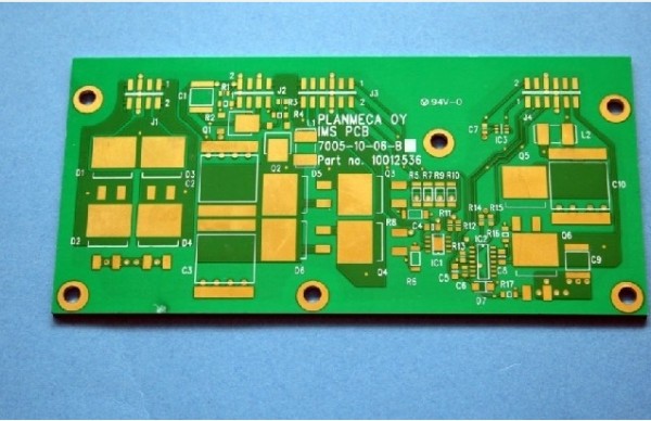
The solder mask layer refers to the part of the PCB covered by ink. Since most PCBs use green ink, the visible green ink part is the solder mask layer. The solder mask layer plays a very important role during the control of the reflow soldering process.

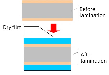
In terms of the solder mask material, it must be applied through a liquid wet process or a dry film lamination. The dry film solder mask material is supplied with a thickness of 0.07 - 0.1mm (0.03 - 0.04″), and it can be suitable for some surface mount products. However, this material is not suitable for PCBs with a relatively close pitch.
The Function of the Solder Mask Layer
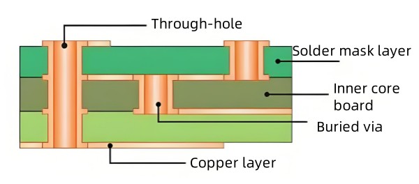
The basic components of a printed circuit board are the pads, vias, solder mask layer, and the text printing part. The solder mask layer is the yellow, red, black, green or other colored part that we can see. Some boards have a yellow solder mask layer. The function of the solder mask layer is to prevent the parts that should not be soldered from being connected by solder, and the reflow soldering is achieved by relying on the solder mask layer. The entire surface of the board passes through the scalding solder. The exposed circuit board without the solder mask layer will be wetted by the solder and soldered, while the part with the solder mask layer will not be wetted by the solder.

The Types of the Solder Mask Layer
The Four Primary Types of the Solder Mask Layer
The solder mask layer can prevent the bridging of conductive solder between various electronic components. In essence, it prevents short circuits. The different PCB solder mask layers are as follows.
• Top and Bottom Mask: Electronic engineers are aware of various openings. They know what is added through ink, epoxy resin or film technology. Then, they can solder the component pins on the board with the help of the determined positions. The conductive trace pattern on the top of the circuit board can also be noticed. These are called top traces. The lower one is the bottom mask.
• Epoxy Liquid: If you want an inexpensive option, choose the epoxy liquid. Thermosetting polymers have a variety of applications. Screen printing is a printing technology. It uses a woven mesh to support the ink-resisting pattern. The mesh can create an open area for the transfer of the ink.
• Photodefinable Liquid Ink: We provide the solder mask layer as an ink formulation. The ink can be sprayed onto the PCB. Then, the pattern can be exposed and developed. It should be noted that this process and the liquid ink formulation are used. This requires a clean environment without pollutants and particles. People can remove it after exposing it to ultraviolet light. This is done by a high-pressure water spray called a developer.
• Photodefinable Dry Film: This solder mask layer is applied by means of vacuum lamination. After the development is completed, you can create openings and solder the components to the copper pads. In addition, tin is used to protect the copper circuit. Then, the dry film is removed.

The Color of the Solder Mask Layer
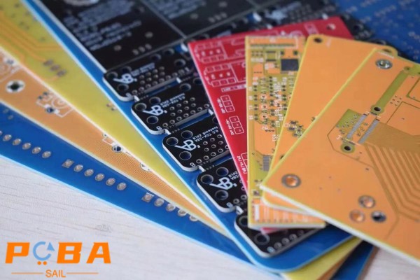
There are many colors on the surface of the PCB. The most common one is green, and black, white and blue are also relatively common. Many people will judge the quality of the PCB according to the color of the ink. Objectively speaking, this judgment standard is inaccurate. There is no direct relationship between the color of the ink and the performance of the circuit board.

The color of the PCB ink can be freely selected according to the customer's needs, and the prices of inks of different colors are also different. The most common green ink has a moderate price and stable quality, which is also the reason why green ink is used the most. The prices of black ink, red ink and white ink are similar, but they are all more expensive than green ink. Yellow ink and purple ink are relatively rare, and their prices are much higher than those of other colors.
In practical applications, green ink is the most widely used. Its process is the simplest and most mature, and it has the longest history. Generally speaking, the board has to go through two processes: board making and chip mounting. Among them, there are several processes in the board making process that have to go through the yellow light room. In this process, the visual effect of green ink is better than that of other colors. In addition, SMT soldering has to go through processes such as soldering and chip mounting, and these processes all require optical positioning and calibration. The green background has a better recognition effect in the instrument, and relatively speaking, it is the least harmful to the eyes.
Since blue ink and black ink contain cobalt and carbon respectively, they have a certain conductivity, so there is a risk of short circuits. While green ink is environmentally friendly, it will not release toxic gases when used in a high-temperature environment. In addition, too dark a color will increase the difficulty of inspection and maintenance of the PCB. For example, black ink is most likely to cause color differences, and generally PCB manufacturers will not easily use black ink. In addition, light-colored inks also have disadvantages. Inks with too light a color can easily show the unsightly appearance caused by operational errors after the via-filling process.
The reason why there are so many colors of PCB inks is not only due to the different qualities of the inks themselves, but also because of their different functional effects. How to choose specifically? It still depends on your own needs.


