


PCB Capabilities
PCBA Capabilities

PCBASAIL always considers customers and makes all invisible things transparent and concrete, including our PCB price structure, the production year and brand of BOM components used, and all details of PCB patch assembly to gain the trust of customers.
Below we will introduce how PCBASAIL produces PCB boards step by step. Understanding the PCB manufacturing process not only allows customers to have a clear understanding of the production progress of their orders, but also allows customers to promptly remedy problems with PCB data to reduce customer losses. Each factory has its own specific processes, but the main manufacturing processes are essentially the same. Due to the complexity of the steps, the related processes for the inner layer of the multilayer board are simplified here.
-
Pre-engineering
-
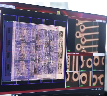
Photo tools
-
Material Cutting
-
Drilling
-
Electroless copper deposition
-
Inner/Outer Imaging
-
Solder Mask
-
Surface Finish
-
AOI Inspection
-
Silkscreen
-
Profiling
-
Electrical test
-
FQC
-
Packing
Step 1. Front-end tool data preparation --- DFM
After receiving the customer's PCB data, the original data will be output into a standard data format (usually Gerber, RS274X extension). This file format clearly defines the data of each layer, including the outline layer, solder mask layer, and silk screen layer. , line layer, drilling, etc., our engineers will check these data to ensure production compliance, and any abnormal data will be fed back to our customers as soon as possible to avoid losses.
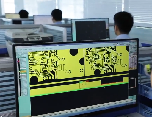
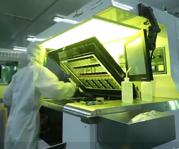
Step 2. Preparing the phototools for PcB image transfer
In a special working environment, the PCB data is transferred to the PCB film used for production at a ratio of 1:1 through a laser photo plotter. The precise scaling configuration of the electronic data directly affects the quality of the final product.
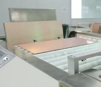
Step 3.Material Cutting
First, we need to select a copper-clad laminate that meets the customer's process requirements and cut it into the size that needs to be processed by an automatic cutting machine.
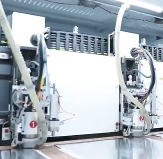
Step 4.Drilling
Drilling is to drill the required via holes in the copper-clad board to provide electrical connections and fix components. If the operation is improper and there is a problem with the via hole process, the device cannot be fixed on the circuit board, which may affect the use at best, or the entire board will be scrapped. At present, there are generally three types of drilling processes.
1. Via hole (VIA)
Copper foil traces that conduct or connect conductive patterns in different layers of a circuit board, but cannot be inserted into copper-plated holes of component leads or other reinforcing materials.
2. Blind hole
The outermost circuit in the PCB is connected to the adjacent inner layer with a plated hole. Because the opposite side cannot be seen, it is called a blind hole. In order to increase the space utilization between PCB circuit layers, blind holes are used, that is, to A via hole on one surface of a printed board.
3. Buried vias
It is a link between any circuit layers inside the PCB but does not lead to the outer layer, and it also means a via hole that does not extend to the surface of the circuit board
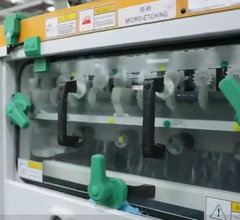
Step 5.Electroless copper deposition
Automatic copper deposition line: chemically deposits a very thin layer of copper on the walls of PCB insulating holes to ensure electrical continuity between layers and through holes. After plating the copper, to optimize the amount of copper to be plated and etched, we also need to plate 25 microns of copper on the vias and 25 – 30 microns of copper on the traces and pads. to meet routing and clearance requirements.
Step 6.Inner/outer imaging
We use photosensitive dry film for image transfer, which is then exposed to a UV light source. Utilizing the photosensitive properties of chemical photosensitive dry films, the mask in the unsensitized areas is removed through development.This forms a negative of the circuit pattern. Then through an etching process, the copper in all areas not covered by the dry film is removed, thereby retaining the copper we need.
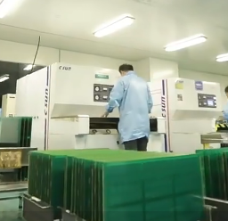
Step 7.Solder mask
Solder resist ink is applied to the entire PCB surface, leaving the through holes and pads on the board to be soldered, covering all lines and copper surfaces to prevent short circuits caused by wave soldering.
Step 8.Surface finish
In order to protect the surface and ensure good solderability, we will treat the surface of the exposed copper area (the pads and holes without solder mask windows), mainly including electroless nickel immersion gold plating, spray tin, immersion silver, etc. And perform thickness and solderability tests.
Step 9.AOI Inspection
AOI detection can fundamentally solve circuit problems such as open, short circuit, micro-open, micro-short etc.
Step10. Silkscreen.
Character silk screen is a kind of identification mark. Silk screen can help us quickly and accurately determine the location of each electronic component on the PCB, and understand the PCB's project name, version information, production date, etc. We image characters and patterns directly from the silk screen layer data of the circuit board. The PCB is then baked to form the characters.
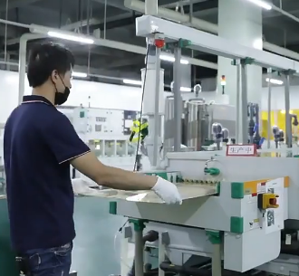
Step11. Profiling.
We cut the panels to specific sizes and shapes based on drilling and profile and mechanical layer files provided by the customer. Cut into veneers of different sizes using V-shaped cutting or CNC, Rounting, etc.
Step12. Electrical test.
We perform electrical testing on every PCB board we produce. Regardless of prototype or batch, ensure that the PCB is open or short-circuited by checking the integrity of the traces and through-hole interconnections. There are two main testing methods, sample: flying probe test, batch: test fixture.
Step13. FQC.
In addition to electrical testing, our professional inspectors will also inspect all PCBs using manual visual inspection and AVI to ensure that all PCBs comply with IPC class II standards and are made in compliance with production requirements, including size, thickness, tolerance,solderability etc., and issue a shipping inspection report (COC documents).
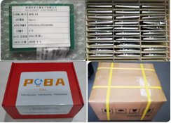
Step14. Packaging&Shipping.
Our circuit boards will be uniformly packaged using vacuum shrink packaging with desiccant to prevent the PCB from moisture and oxidation. Other required materials such as PCB test coupons, COC documents, etc. will also be provided together with the PCB and sent to the customer via international express delivery such as DHL, UPS, Fedex, etc.