Fundamental Definition: What is a Ceramic PCB?
Broadly, "industrial ceramic products" refer to items made by firing raw materials like clay—this category also includes glass and cement products processed via high-temperature furnace firing.
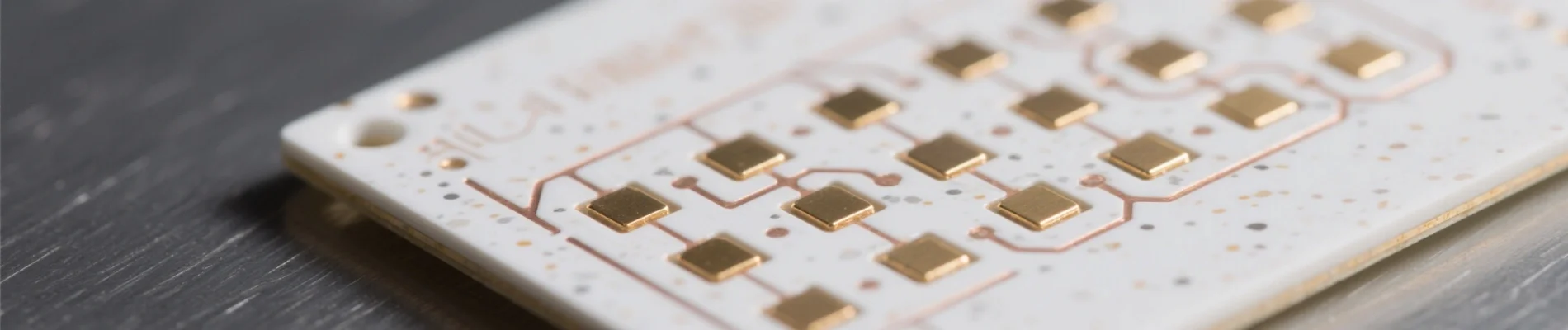
By definition, a substrate is a component that physically protects a chip while enabling electrical connections between the chip and external components. A ceramic PCB, as the name implies, is a specialized circuit board where the substrate is crafted from ceramic materials.
Specifically, a ceramic PCB is manufactured by directly bonding copper foil (single-sided or double-sided) to the surface of a ceramic base material—typically alumina (Al₂O₃) or aluminum nitride (AlN)—using high-temperature processes. The result is an ultra-thin composite substrate with exceptional electrical insulation, high thermal conductivity, superior solderability, and strong interlayer adhesion. Like traditional printed circuit boards (PCBs), it can be precision-etched into complex patterns and supports high current loads. These properties make ceramic PCBs a foundational material for high-power electronic circuit design and advanced interconnection technologies.
Ceramic PCB PCBs: Core Characteristics
A ceramic PCB is a high-performance circuit board produced by bonding copper foil directly to an alumina (Al₂O₃) or aluminum nitride (AlN) ceramic base at elevated temperatures, with options for single-sided or double-sided copper layers. This manufacturing process yields an ultra-thin composite structure that excels in key areas:
- Excellent electrical insulation to prevent short circuits;
- High thermal conductivity for efficient heat dissipation;
- Strong solderability for reliable component attachment;
- Robust adhesion between copper and ceramic layers.
Like traditional PCBs, it can be etched into intricate circuit patterns and handles high current flows effectively. As a result, ceramic PCBs have become indispensable in high-power electronic systems, serving as a critical foundation for circuit structure and interconnection technologies.
Comparative Analysis: Ceramic vs. Traditional Substrates
Differences Between Ceramic Substrates and PCBs
Material composition
Ceramic substrates are inorganic, with cores made of materials like alumina (Al₂O₃) or aluminum nitride (AlN). In contrast, traditional PCBs use organic materials such as FR-4 (fiberglass-reinforced epoxy resin). Ceramic substrates are inherently brittle and (in most cases) cannot be laminated into multi-layer structures, whereas traditional PCBs offer design flexibility, including multi-layer lamination.
Performance and applications
Ceramic substrates are engineered for industries with stringent heat dissipation requirements, such as high-power LED lighting (where excess heat reduces efficiency), high-power modules, high-frequency communication systems, and railway power supplies. Traditional PCBs, meanwhile, find broader use in consumer electronics, commercial devices, and everyday electrical equipment.
Performance Metrics Comparison
Based on industry standard testing data
| Characteristics | Ceramic Substrates | Traditional PCBs (FR4) |
|---|---|---|
| Material Composition | Inorganic (Al₂O₃, AlN) | Organic (fiberglass reinforced resin) |
| Thermal Conductivity | 15–230 W/mK | 0.2–0.4 W/mK |
| Electrical Insulation | Excellent (20 kV/mm breakdown voltage) | Good (10–15 kV/mm breakdown voltage) |
| Mechanical Properties | High strength, brittle | Flexible, lower strength |
| Cost | High | Low |
| High Frequency Performance | Excellent | Good (limited by resin) |
Specialized Comparison: Ceramic vs. High-Frequency Boards
Base Material Differences
Ceramic substrates derive their core properties from alumina (Al₂O₃) or aluminum nitride (AlN), delivering exceptional thermal management performance. In contrast, high-frequency PCBs typically use materials such as Rogers, Arlon, or polytetrafluoroethylene (PTFE)—materials that prioritize signal integrity over thermal performance.
These high-frequency materials feature low dielectric constants and dielectric loss factors, enabling efficient signal transmission in high-frequency communication applications (1 GHz and above), where maintaining signal integrity is critical.
Key Application Differences
- Ceramic Substrates:High-power electronic applications, LED lighting, power modules, aerospace electronics
- High-Frequency Boards: RF (radio frequency) communication, radar systems, microwave technologies, 5G infrastructure
- Overlap Areas: Some advanced communication systems require both high-frequency performance and thermal management, often utilizing hybrid solutions that combine elements of both substrate types.
Performance Profile: Advantages & Limitations
Key Advantages
-
High resistance
Provides strong electrical resistance, making it suitable for applications requiring stable insulation.
-
Excellent high-frequency performance
Maintains signal integrity even in high-frequency environments, ideal for communication and radar systems.
-
High thermal conductivity
Outperforms metals and resins in heat transfer due to inherent material properties, critical for dissipating heat in high-power devices.
-
Superior chemical stability
Resists vibration, extreme temperatures, and pressure. Internal circuits and alignment markers (MARK points) are more durable than those on conventional substrates.
-
Precision in manufacturing
Ensures accuracy in printing, component mounting, and soldering processes, reducing assembly errors.
Ensures accuracy in printing, component mounting, and soldering processes, reducing assembly errors.
-
No organic components
Resistant to cosmic radiation, enhancing reliability and extending service life in aerospace and high-reliability applications.
-
Oxide-free copper layers
The copper foil used in ceramic substrates lacks oxide layers, allowing long-term use in reducing atmospheres without degradation.
Key Limitations
-
Fragility
Ceramic materials are inherently brittle, limiting production to small-area circuit boards and requiring careful handling to avoid breakage.
-
High cost
Manufacturing ceramic substrates involves complex processes and specialized materials, making them more expensive than standard PCBs. This restricts their use to high-end applications, as low-cost consumer products rarely justify the expense.
-
Production limitations
Difficult to produce in large sizes due to material properties and manufacturing constraints, limiting application scope.
-
Processing challenges
Requires specialized equipment and techniques for cutting, drilling, and shaping, increasing manufacturing complexity.

Material Classifications & Properties
Alumina
The most widely used ceramic PCB material, offering a balance of performance and cost. High mechanical strength and excellent thermal stability make it suitable for diverse applications. Leading manufacturers like Siliton now offer 3D-customized alumina substrates, expanding their use in complex designs.
Aluminum Nitride
Offers high thermal conductivity and a thermal expansion coefficient that closely matches silicon (Si), reducing stress in chip-substrate bonding. A notable drawback is their sensitivity to surface oxidation—even a thin oxide layer can reduce thermal conductivity. Currently, few domestic manufacturers (such as Siliton) have mastered large-scale production of AlN substrates.
Beryllium Oxide
Boasts the highest thermal conductivity but is toxic, restricting use to specialized, low-volume scenarios. Thermal performance drops significantly above 300°C.
Classified by Manufacturing Process
Common ceramic heat-dissipation substrates include HTCC, LTCC, DBC, DPC, and LAM. Among these, LAM is a patented technology developed by Siliton in collaboration with the National Optoelectronics Laboratory at Huazhong University of Science and Technology. HTCC and LTCC involve sintering processes, which contribute to their higher costs. DBC and DPC have matured in China in recent years, enabling mass production, while LAM (laser activation metallization) represents an innovative advancement in the field.
High-Temperature Co-fired Ceramic
HTCC shares similarities with LTCC but uses ceramic powder without glass additives. The manufacturing process begins with forming "green sheets" (unfired ceramic layers) that are sintered at extremely high temperatures (1300–1600°C) to harden.
Via holes are drilled into these sheets to enable layer-to-layer communication, then filled with conductive materials using screen printing. Due to the high sintering temperature, conductors are limited to high-melting metals like tungsten, molybdenum, or manganese. Layers are stacked and co-fired to form the final multi-layer substrate.
Low-Temperature Co-fired Ceramic
LTCC substrates are produced by mixing inorganic alumina powder with 30–50% glass powder and organic binders to create a slurry. This slurry is cast into thin sheets, which are dried to form flexible green sheets.
Via holes are drilled into these sheets for interlayer connections, and conductive pastes (using metals like silver, copper, or gold) are applied via screen printing. Layers are stacked and sintered at lower temperatures (850–900°C), allowing the use of more conductive metals.
Direct Bonded Copper
DBC technology bonds copper foil directly to ceramic substrates using a copper-oxygen eutectic reaction. During manufacturing, controlled amounts of oxygen are introduced between the copper and ceramic layers.
At temperatures between 1065°C and 1083°C, copper and oxygen form a Cu-O eutectic liquid that reacts with the ceramic PCB to create a strong interfacial layer (CuAlO₂ or CuAl₂O₄) while wetting the copper foil, resulting in a robust bond.
Direct Plate Copper
DPC begins with cleaning and preparing the ceramic PCB. A thin copper composite layer is deposited onto the ceramic surface using vacuum sputtering—a precision thin-film technology.
Photolithography is then used to pattern circuits: photoresist is applied, exposed to UV light through a mask, developed to reveal the circuit pattern, and etched to remove unwanted copper. The remaining copper layer is thickened via electroplating, and the photoresist is stripped.
Laser Activation Metallization – Siliton Technology
LAM uses high-energy laser beams to ionize the surface of ceramic and metal materials, enabling them to bond at a molecular level for exceptional adhesion.
Key features:
- Enhanced thermal conductivity: Alumina ceramics (15–35 W/mK) and AlN ceramics (170–230 W/mK)
- Optimized thermal expansion matching with semiconductor chips
- Strong bonding strength (up to 45 MPa) and low-resistance metal layers (<2.5×10⁻⁶ Ω·cm)
- Superior solderability and high-temperature tolerance
- Exceptional insulation (breakdown voltage up to 20 kV/mm)
- Customizable conductor thickness (1μm to 1mm)
- Low high-frequency loss and high-density assembly (20μm L/S resolutions)
- Organic-free composition and oxide-free copper
- 3D substrates and wiring capability
Thermal Conductivity
Bond Strength
Conductor Thickness Range
LAM Technology: Advanced Features & Benefits
Laser Activation Metallization (LAM) represents an innovative advancement in ceramic PCB manufacturing, developed by Siliton in collaboration with the National Optoelectronics Laboratory at Huazhong University of Science and Technology, offering superior performance characteristics compared to traditional methods:
Enhanced Thermal Conductivity
Alumina ceramics offer 15–35 W/mK and AlN ceramics 170–230 W/mK, significantly outperforming traditional aluminum-based PCBs (1–2 W/mK).
Optimized Thermal Expansion Matching
Ceramic's thermal expansion coefficient closely matches that of semiconductor chips, preventing solder joint failure during temperature changes (common in high-power LEDs operating at 80–90°C).
Strong, Low-Resistance Metal Layers
Metal-ceramic bonding strength reaches up to 45 MPa (exceeding the strength of 1mm-thick ceramic), while copper layers achieve volume resistivities <2.5×10⁻⁶ Ω·cm to minimize energy loss.
Superior Design Flexibility
Achieves line/spacing (L/S) resolutions of 20μm for miniaturization, with customizable conductor thickness from 1μm to 1mm and unique 3D substrate capabilities.
Technology Assessment & Future Outlook
While LTCC, HTCC, DBC, DPC, and LAM ceramic substrates are all widely researched and used, LAM technology stands out as the most promising solution for high-power LED heat dissipation applications, thanks to its superior thermal performance, design flexibility, and manufacturing versatility.
Ceramic substrates provide critical advantages in high-power, high-frequency, and high-reliability applications where traditional PCB materials fall short. Their exceptional thermal conductivity, electrical insulation, and chemical stability make them indispensable in advanced electronic systems, despite their higher cost and manufacturing complexity. Ongoing advancements in manufacturing processes, particularly with LAM technology, are expected to expand their applications and reduce cost barriers.
Need Ceramic PCB?
Our team of experts can provide technical guidance on ceramic PCB selection, design, and manufacturing processes tailored to your specific application requirements.