PCB Assembly Quality: Key Processes & Common Fixes
 24 Apr 2025 11:39:52 GMT
PCBASAIL
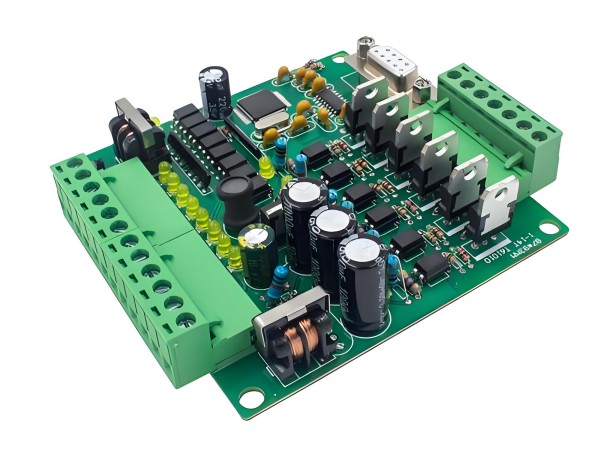
In the electronics industry, PCB (printed circuit board) assembly is a key step in transforming the design of components into actual functional circuits. Each process of assembly will have a great impact on the performance of electronic products. Each component includes capacitors, resistors, crystal oscillators, chips, diodes, transistors, transformers, switches, fuses, etc. From bare board PCB to PCBA, achieving the performance and reliability of functional circuits is related to its PCB assembly process and technology. Now, let's explore how PCB assembly actually works and fix typical problems.
I. Basic types of PCB
1.1 Single-sided PCB
Single-sided PCB is the most basic type of PCB. This design structure is relatively simple, and all electronic components are installed on the same side.
1.2 Double-sided PCB
Double-sided PCB has conductive lines on both the upper and lower sides, which is suitable for more complex circuit designs. The electrical connection of the two-sided lines is achieved through vias.
1.3 Multilayer PCB
Multilayer PCB is mainly composed of three or more conductive layers and insulating layers stacked alternately, usually including power layer, ground layer and signal layer. The manufacturing process of this multilayer PCB is complex and has high requirements for production equipment and technology.
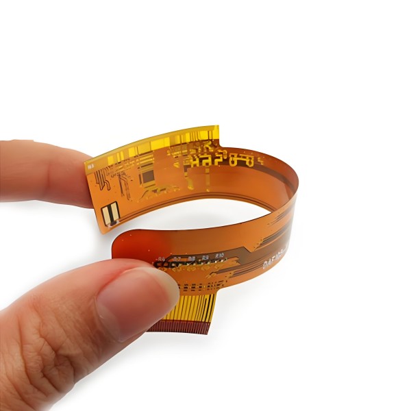
1.4 Flexible PCB (FRC)
Flexible PCB is mainly based on flexible insulating materials, such as polyimide (PI), which has the characteristics of being bendable, foldable and winding. This kind of FRC can adapt to various complex spatial structures.
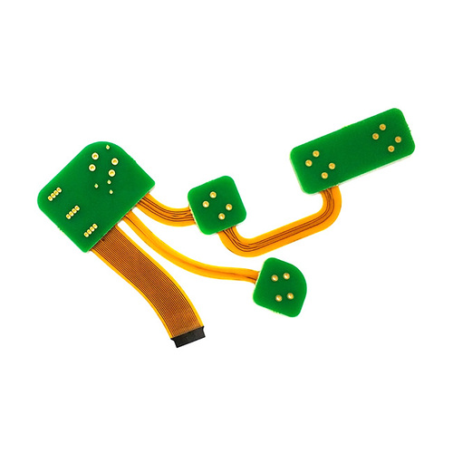
1.5 Rigid-Flex PCB
Rigid-Flex PCB combines the advantages of rigid PCB and flexible PCB, and its design and manufacturing are relatively difficult.
II. PCB assembly production process
2.1 Inspection of components and bare PCB boards
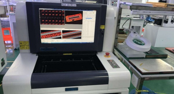
Before assembling the materials, all components and bare PCB boards need to be inspected. Carefully check the specification and quantity according to the BOM (Bill of Materials), check whether the appearance is damaged, whether the pins are oxidized or deformed. LEDs will also use a multimeter to check whether the components are working properly. For bare PCB boards, check whether the circuits are complete without open circuits or short circuits, whether the vias are blocked, whether the solder mask and silk screen layers on the surface are clear and accurate, and use AOI (Automatic Optical Inspection) equipment to ensure that the bare board meets the assembly requirements.
2.2 Tools and Equipment Debugging
Prepare the tools and equipment needed for assembly, calibrate the accuracy and visual recognition system of the placement machine to ensure that tiny components can be accurately grasped and placed; also need to debug the temperature, transmission speed and other parameters of the reflow and wave soldering furnaces to meet the welding process requirements; check the status of the electric soldering iron and soldering head to ensure welding operation.
2.3 First piece verification and process confirmation
First, produce the first sample (1-2 PCBs) according to the debugged equipment and process. Secondly, visually check whether the component mounting position and polarity are correct, whether the solder joints are full, and use AOI/SPI to check the solder paste and component mounting quality. Perform a comprehensive inspection of the first piece.
Ⅲ. Soldering methods
3.1. Reflow soldering
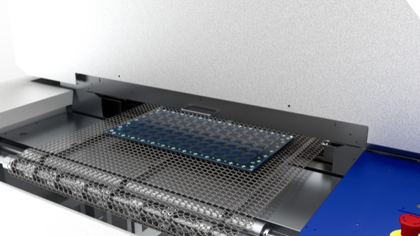
The solder paste (containing solder particles + flux) is melted by heating to form an alloy layer (metallurgical bonding) between the component pins and the pads.
It is necessary to ensure that the lead-free solder paste temperature is sufficient, but avoid excessive temperature or high temperature for too long, which may cause carbonization of components or coking of PCB substrate, resulting in invisible open circuits. At the same time, if the opening of the steel mesh is too large, it is easy to cause bridge short circuits due to excessive amount of solder paste, and if the opening is too small, it will cause cold welding due to insufficient solder.
3.2. Wave soldering
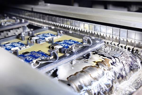
PCB contacts the molten solder wave to achieve through-hole component welding.
If the temperature of wave soldering is too high, the solder will flow to the component surface, causing short circuits between components. If the temperature is too low, the solder will not climb enough, resulting in separation of the pin pads (false soldering). At the same time, the amount of flux sprayed should be avoided to avoid insufficient welding, resulting in non-wetting, and excessive residue will lead to electrochemical corrosion in the later stage.
3.3 Manual Soldering
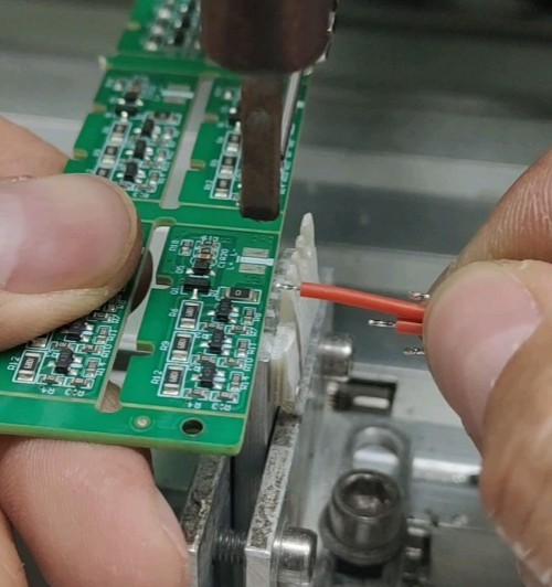
Manually use a soldering iron to heat the solder joint and add solder wire to complete the connection.
When manually soldering, if the temperature is lower than 300°C or the time is shorter than 2 seconds, the solder will not be fully wetted and a cold solder joint will be formed. If the temperature is higher than 400°C or the time exceeds 5 seconds, it is easy to burn the components or cause the pad to fall off, resulting in a permanent open circuit. In addition, if the diameter of the solder wire is too thick, it is easy to cause bridging between pads. While insufficient solder lead to weak joints due to imcomplete fillet formation.
Ⅳ.PCB Assembly Common Issues and Solutions
4.1 Open Circuit
4.1.1 Phenomenon:
Solder fails to form a reliable metallurgical bond, causing intermittent or complete disconnection.
4.2.2 Solution:
Ensure solder paste is properly thawed and mixed to avoid moisture and absorption; Regularly consistent solder paste thickness and clean stencils;Adjust temperature profile to ensure sufficient heat for proper wetting.
4.2 Short Circuit
4.2.1 Phenomenon:
Excess solder connects adjacent pads or circuits, leading to current leakage or component failure.
4.2.2 Solution:
Reduce the amount of solder paste for dense-foot components to avoid overprinting or collapse. For tiny components, use a high-precision placement machine, and strictly align the polarity component direction with the silk screen logo. Adjust the wind speed and height of welding to accelerate the solidification of solder joints and avoid overflow. In the dense pad spacing, the solder mask layer adds an anti-bridge dam design. In order to prevent solder paste accumulation, the steel mesh window design is smaller than the pad. After printing, clean the residual solder paste on the bottom of the steel mesh in time.
V. Summary
In short, PCB assembly is a complex and delicate process, and it is also an indispensable part of modern electronic manufacturing. Striving for excellence in every step can we create high-quality and high-reliability PCB. Through standardized processes, precise process control and advanced detection technology, the defect rate can be significantly reduced to ensure high performance and high reliability.
To meet your needs, you need a PCB factory with the following qualities:
(1) They can optimize soldering and inspection solutions based on requirements to improve yield rates.
(2) To ensure precision control from component selection and soldering processes to quality inspection.
(3) Provide clear quotation details, including BOM(Bill of Materials) costs, PCB fabrication, and assembly costs.
Are you looking for a PCB assembly supplier? Please feel free to provide information such as the board layers, component lists, process requirements, ect.
PCBASAIL is your reliable supplier.


