Rigid-Flex PCBs: Materials and Design Requirements
 11 Apr 2025 11:12:10 GMT
PCBASAIL
Table of Contents1. What is a rigid-flex printed circuit board?2. Common Structures of Rigid-Flex Printed PCB3. The Production Process of Rigid-Flex Printed Circuit Boards4. Wiring Requirements for Rigid-Flex Printed Circuit Boards
In electronic device manufacturing, the rigid-flex printed circuit board is a special board. It is used in many high-end electronic products. It mixes the strength of a printed circuit board with the bend of a flexible printed circuit and gives design benefits.
What is a rigid-flex printed circuit board?
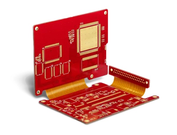
A rigid-flex printed circuit board is a special board made by joining a hard board and a bendable board using set methods. It keeps the good traits of the hard board—like high strength, high reliability, and multi-layer wiring—and gives the board the ability to bend and fold in some areas. This type of board is used when saving space, high integration, stronger product quality, and flexibility are needed. The main materials are the hard material FR4 and the flexible material polyimide (PI). FR4 gives strength and electrical insulation, and PI provides bendability and heat resistance. They are put together by lamination to form a special board.

Common Structures of Rigid-Flex Printed PCB
The design of these boards is simple and can change to meet different needs. Here are some common types:
1. Reinforced Concrete Structure (Analogy): The design is like reinforced concrete. The rigid part (such as FR4) gives strength, and the flexible part (such as PI) gives bend. Both parts work together.
2. Steel Structure: In some cases, the board uses a design like a steel structure. The rigid area is made of steel or another strong material, and the flexible area stays the same. This design is light, quick to make, and can be recycled.
3. Wood Structure: In some light or temporary electronic devices, the board might use a wood structure to support the flexible area. This case is rare. The board with a wood structure is light and holds heat well.
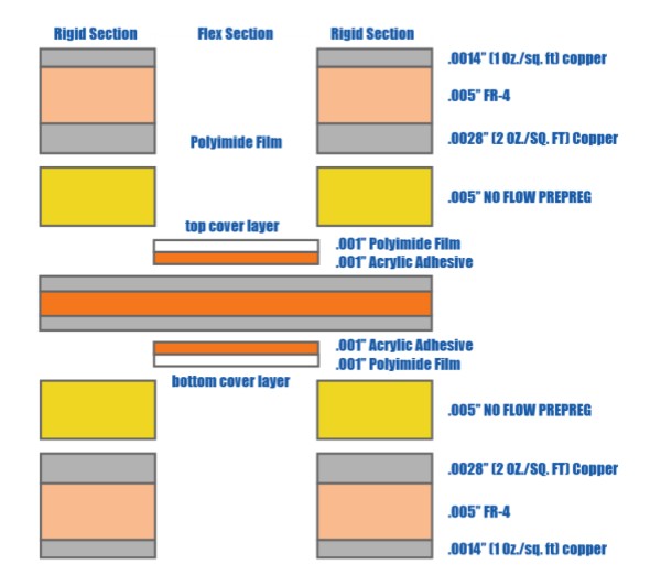
4. Composite Structure: The most common design is composite. For example, a board may include a double-layer flexible substrate, gold fingers, two layers of hard board, and an FR4 filling layer. The parts match to give both strength and bend.

The Production Process of Rigid-Flex Printed Circuit Boards
The making of these boards is complex and needs careful work. An error in one step can affect the final quality. A typical process is:
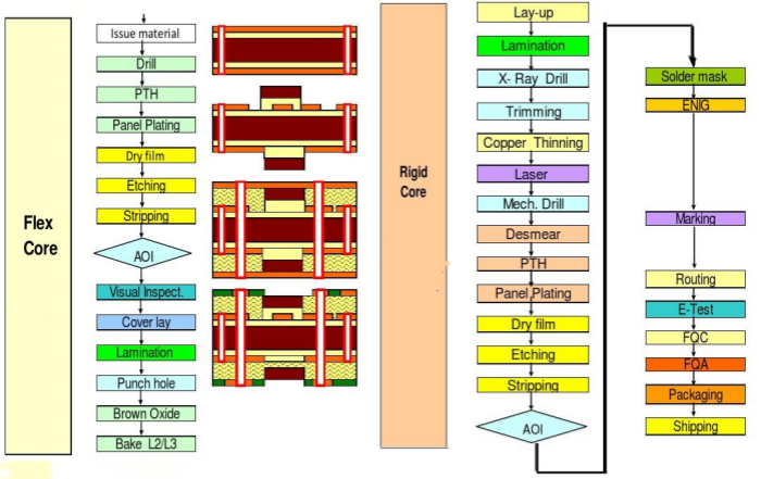
1. Material Cutting and Drilling: First, cut and drill the FR4 and PI materials as needed. It is important to control the size and position.
2. Laminating Dry Film and Exposure: Next, put the dry film on the copper-clad material and expose it to form the needed circuit pattern. Then, remove extra copper using development and etching to form a basic board.
3. Combining the Flexible Board and the Rigid Board: Then, put the flexible FPC board and the hard PCB board together. They are aligned and laminated. This is a key step that needs careful control to stop bubbles and empty spots.
4. Subsequent Processing: After lamination, the board is trimmed, drilled, cleaned of adhesive residues, and then copper is deposited and electroplated. These steps help make the board work well both electrically and mechanically.
5. Surface Treatment and Inspection: Finally, the board gets surface treatment such as solder resist printing and marking. The board is tested electrically and checked for appearance. Only the good boards are sent to customers.

The Production Difficulties and Advantages of Rigid-Flex Printed Circuit Boards
Making these boards is hard. First, different material traits make processing difficult. Second, the complex design needs careful control. Third, many steps are needed, and the yield is low. The advantages are clear:
Space Saving: The three-dimensional assembly saves space.
Performance Improvement: The mix of strength and bend improves overall performance.
Enhanced Flexibility: They do well when bending and folding are needed.
Weight Reduction: They are usually lighter than traditional multi-layer PCBs.
Materials for Multi-layer Rigid-Flex Printed Circuit Boards
Required Materials | Traditional Materials | High-performance Materials |
Flexible Circuit Copper Clad Laminate (FCCL) | Traditional Polyimide Film | New-type Polyimide Film |
Double-sided Copper Clad Laminate | Polyimide Substrate, Acrylic Adhesive (Epoxy Adhesive) | Adhesive-free Polyimide Substrate Laminate (Cast or Laminated Type) |
Coverlay | Traditional Polyimide Coated with Acrylic or Epoxy Resin Adhesive | New-type Polyimide Coated with Hot-melt Polyimide Adhesive |
Bonding Sheet | Acrylic Resin Adhesive Film, Epoxy Resin Adhesive Film, Polyimide Film Coated with Acrylic Adhesive on Both Sides | New-type Polyimide Film Coated with Hot-melt Polyimide Resin on Both Sides |
Rigid Circuit Copper Clad Laminate (CCL) | Glass-Epoxy Resin | Glass-BT Resin Board, Glass-Polyimide Resin Board |
The table shows some materials used in making rigid-flex printed circuit boards. As technology gets better, these materials work much better. The materials must stand high heat and keep their shape when heated. In high-reliability fields like the military and space, a thick polyamide film (more than 50um) is advised. The board must be stable and strong when made. In consumer electronics, the trend is to make things thin, light, and small. So a thin material (less than 50um) is usually used. For adhesive copper clad laminates, coverlays, and bonding sheets, using acrylic adhesives gives strong bonding. Yet, it does not stand heat well and shrinks more. Epoxy adhesives stand heat better. Yet, they take longer to set and bond less strongly. Copper clad laminate boards without adhesive, made by casting or lamination, can stand heat better and do not expand as much. They can also make the final product thinner. Special equipment and process conditions are needed for these materials because they must be processed at over 300°C.
Layout Requirements for Rigid-Flex Printed Circuit Boards
a. Put the components in the hard area. Use the flexible area only for connection. This way, the bending life is long and the board works well. If the components go in the flexible area, the pads may break or the markings may come off.
b. When you put the components in the hard area, leave more than 1mm between the edge of the component and where the hard and flexible areas meet.
c. If the flexible area goes into the hard area, leave at least 1mm between them.

Wiring Requirements for Rigid-Flex Printed Circuit Boards
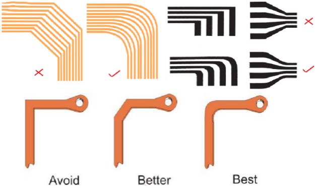
a. Make the circuit lines in the flexible area go across the bending line. At the bending part, shape the circuit line in an arc to stop it from breaking when bent.
b. Keep the circuit line at least 10mil away from the board edge in the flexible area and do not drill holes there. Leave at least 2mm between the via hole and where the hard and flexible areas meet.
c. If there is a hidden electrical layer in the flexible area, put isolation there. This does not affect the power, current, or impedance and helps keep the flexible area bendy.
d. To tell the flexible area apart during making, add a mark on the flexible area of the mechanical layer.
e. If the design needs impedance control and impedance lines go into the flexible area, make sure that each wiring layer there has a matching reference layer.


