Flexible PCBs: Basics, Materials and Limitations
 03 Apr 2025 16:47:58 GMT
PCBASAIL
What is a Flexible Printed Circuit Board?
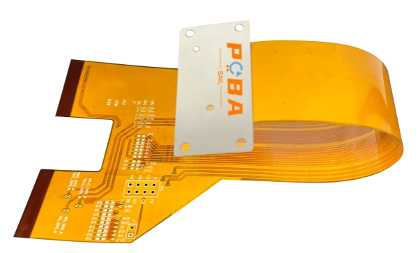
With the rapid development of electronic products, there are many types of circuit boards, including rigid boards, flexible pcb board, and rigid-flex boards. A rigid board is a common PCB board that cannot be bent. The vast majority of products use rigid boards. A flexible board, also known as a flexible printed circuit (FPC), whose full name is Flexible Printed Circuit Board (abbreviated as FPC). It is a printed circuit board made of flexible insulating substrates such as polyimide or polyester film. PCB flexible boards have the characteristics of being bendable, foldable, and coiled, and can meet the design requirements of complex shapes. They are widely used in mobile devices, automotive electronics, medical devices, and other fields. A rigid-flex board contains both rigid and flexible parts.
Classification of Flexible PCBs
Flexible PCBs are usually classified according to the number of conductor layers and their structure as follows:
1.1 Single - sided Flexible PCB
A single - sided flexible PCB has only one conductor layer. Its surface may or may not have a cover layer. The insulating base materials used vary depending on the product's application. Commonly used insulating materials generally include polyester, polyimide, polytetrafluoroethylene, and flexible epoxy - glass cloth.
Single - sided flexible PCBs can be further divided into the following four categories:
1. Single - sided connected without a cover layer: In this type of flexible PCB, the conductor pattern is on the insulating substrate, and there is no cover layer on the conductor surface. It is similar to a common single - sided rigid PCB. This type of product is the cheapest and is usually used in non - critical applications with environmental protection requirements. Its interconnections are achieved by soldering, fusion welding, or pressure welding. It was commonly used in early telephones.
2. Single - sided connected with a cover layer: Compared with the previous type, this type has an additional cover layer on the conductor surface according to customer requirements. When covering, the pads need to be exposed. For simple cases, the end area can be left uncovered. For precision requirements, the clearance hole form can be adopted. It is the most widely used type of single - sided flexible PCB and is widely used in automotive instruments and electronic instruments.
3. Double - sided connected without a cover layer: In this type, the connection pads can be connected on both the front and back of the conductor. To achieve this, a via hole is made in the insulating substrate at the pad. This via hole can be made by punching, etching, or other mechanical methods at the required position of the insulating substrate. It is used for the installation of components on both sides and in soldering situations. There is no insulating substrate in the pad area of the via, and this type of pad area is usually removed by chemical methods.
4. Double - sided connected with a cover layer: The difference between this type and the previous one is that there is a cover layer on the surface. The cover layer has via holes, allowing both - side terminations while still maintaining the cover layer. This type of flexible PCB is made of two layers of insulating materials and one layer of metal conductor. It is used in situations where the cover layer needs to be insulated from surrounding devices, the PCB itself needs to be insulated, and both - side connections are required at the ends.
1.2 Double - sided Flexible PCB
A double - sided flexible PCB has two conductor layers. The applications and advantages of this type of double - sided flexible PCB are the same as those of single - sided flexible PCBs. Its main advantage is to increase the wiring density per unit area. It can be classified according to the presence or absence of metallized holes and cover layers into: a) without metallized holes and without a cover layer; b) without metallized holes and with a cover layer; c) with metallized holes and without a cover layer; d) with metallized holes and with a cover layer. Double - sided flexible PCBs without cover layers are less commonly used.
1.3 Multilayer Flexible PCB
Similar to rigid multilayer PCBs, flexible multilayer PCBs can be made using multi - layer lamination technology. The simplest flexible multilayer PCB is a three - layer flexible PCB formed by covering two layers of copper shielding layers on both sides of a single - sided PCB. This three - layer flexible PCB is electrically equivalent to coaxial or shielded wires. The most commonly used structure of flexible multilayer PCBs is a four - layer structure, with interlayer interconnections achieved through metallized holes. The middle two layers are generally the power layer and the ground layer.
The advantages of flexible multilayer PCBs are that the base film is lightweight and has excellent electrical properties, such as a low dielectric constant. A flexible multilayer PCB board made of polyimide film as the base material is about 1/3 lighter than a rigid epoxy - glass cloth multilayer PCB board. However, it loses the excellent flexibility of single - sided and double - sided flexible PCBs. Most such products do not require flexibility.
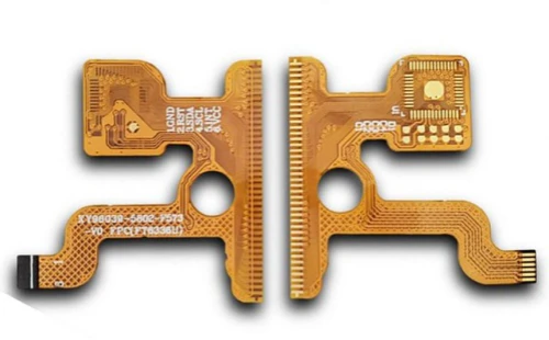
Flexible multilayer PCBs can be further divided into the following types:
1. Multilayer PCBs formed on flexible insulating substrates with specified flexibility in the finished product: This structure usually bonds the two - side ends of many single - sided or double - sided microstrip flexible PCBs together, but the central part is not bonded, thus having a high degree of flexibility. To achieve the desired electrical properties, such as matching the characteristic impedance performance with the rigid PCB it interconnects, each circuit layer of the flexible multilayer PCB component must design signal lines on the ground plane. To ensure a high degree of flexibility, a thin and suitable coating, such as polyimide, can be used on the conductor layer instead of a thicker laminated cover layer. Metallized holes enable the required interconnections between the flexible circuit layers in the z - direction. This type of flexible multilayer PCB is most suitable for designs that require flexibility, high reliability, and high density.
2. Multilayer PCBs formed on flexible insulating substrates with no specified flexibility in the finished product: This type of flexible multilayer PCB is made by laminating flexible insulating materials, such as polyimide film, into a multilayer board. After lamination, it loses its inherent flexibility. When the design requires maximizing the use of the insulating properties of the film, such as a low dielectric constant, a uniform - thickness medium, light weight, and continuous - processing ability, this type of flexible PCB is used. For example, a multilayer PCB made of polyimide film insulating material is about one - third lighter than a rigid epoxy - glass cloth PCB.
3. Multilayer PCBs formed on flexible insulating substrates that must be formable but not continuously flexible in the finished product: This type of flexible multilayer PCB is made of flexible insulating materials. Although it is made of flexible materials, due to electrical design limitations, such as requiring thick conductors for the required conductor resistance or thick insulating isolation between the signal layer and the ground layer for the required impedance or capacitance, it is formed during the application of the finished product. The term "formable" is defined as: a flexible multilayer PCB component has the ability to be formed into the required shape and cannot be flexed further during application. It is used in the internal wiring of avionics equipment units. At this time, low - resistance conductors for stripline or three - dimensional space designs, minimal capacitive coupling or circuit noise, and smooth 90° bending at the interconnection ends are required. A flexible multilayer PCB made of polyimide film material can achieve this wiring task because polyimide film has high - temperature resistance, flexibility, and good overall electrical and mechanical properties. To achieve all the interconnections in this component section, the wiring part can be further divided into multiple multilayer flexible circuit components and joined together with adhesive tape to form a printed circuit bundle.
Common Substrate Material Types for Flexible PCBs
Substrate
The most important material in a flexible or rigid PCB is its base substrate material. It is the material on which the entire PCB is based. In rigid PCBs, the substrate material is usually FR - 4. However, in Flex PCBs, the commonly used substrate materials are polyimide (PI) film and PET (polyester) film. In addition, polymer films such as PEN (polyethylene naphthalate), PTFE, and aramid can also be used.
Polyimide (PI), a "thermosetting resin", remains the most commonly used material for Flex PCBs. It has excellent tensile strength, is very stable in a wide operating temperature range from - 200°C to 300°C, has chemical corrosion resistance, excellent electrical properties, high durability, and excellent heat resistance. Unlike other thermosetting resins, it can maintain its elasticity even after thermal polymerization. However, PI resin has disadvantages such as poor tear strength and a high moisture absorption rate. On the other hand, PET (polyester) resin has poor heat resistance, which "makes it unsuitable for direct soldering", but it has good electrical and mechanical properties. Another substrate, PEN, has medium - level properties better than PET but not as good as PI.
Liquid Crystal Polymer (LCP) Substrate
LCP is a substrate material that is rapidly gaining popularity in Flex PCBs. This is because it overcomes the disadvantages of PI substrates while maintaining all the properties of PI. LCP has a moisture resistance and water - repellency of 0.04% and a dielectric constant of 2.85 at 1GHz. This makes it well - known in high - speed digital circuits and high - frequency RF circuits. The molten form of LCP is called TLCP, which can be injection - molded and pressed into flexible PCB substrates and can be easily recycled.
Resin
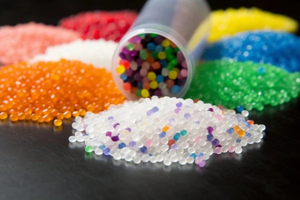
Another material is the resin that tightly bonds the copper foil and the base material together. Resins can be PI resin, PET resin, modified epoxy resin, and acrylic resin. The resin, copper foil (top and bottom), and the substrate form a "sandwich" called a laminate. This laminate is called FCCL (Flexible Copper - Clad Laminate), which is formed by applying high temperature and pressure to the "stack" through automatic pressing in a controlled environment. Among the mentioned resin types, modified epoxy resin and acrylic resin have strong adhesion properties.
These adhesive resins are not conducive to the electrical and thermal properties of Flex PCBs and reduce dimensional stability. These adhesives may also contain halogens harmful to the environment and are restricted by EU regulations. According to these environmental protection regulations, the use of 7 harmful substances is restricted, including lead (Pb), mercury (Hg), cadmium (Cd), hexavalent chromium (Cr 6+), polybrominated biphenyls (PBB), polybrominated diphenyl ethers (PBDE), bis(2 - ethylhexyl) phthalate (DEHP), and butyl benzyl phthalate (BBP).
Therefore, a solution to this problem is to use 2 - layer FCCL without adhesives. 2L FCCL has good electrical properties, high heat resistance, and good dimensional stability, but its manufacturing is difficult and costly.
Copper Foil
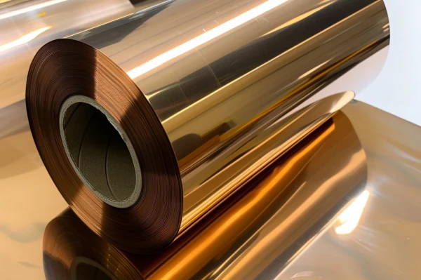
Copper is another top - level material in flexible PCBs. PCB traces, pads, vias, and holes are all filled with copper as a conductive material. We are all aware of the conductive properties of copper, but how to print these copper traces on the PCB remains a topic of discussion. There are two methods of copper deposition on a 2L - FCCL (2 - layer flexible copper - clad laminate) substrate: 1) Electroplating; 2) Lamination. The electroplating method has fewer adhesives, while the laminate contains adhesives.
· Electroplating: In the case of requiring an ultra - thin Flex PCB, the conventional method of laminating copper foil on a PI substrate through a resin adhesive is not suitable. This is because the lamination process has a 3 - layer structure (Cu - Adhesive - PI), making the stacked layer thicker, so it is not recommended for double - sided FCCL. Therefore, another method called "sputtering" is used. In this method, copper is sputtered onto the PI layer through "electroless" plating, either by wet or dry methods. This electroless plating deposits a very thin copper layer (seed layer), and in the next step called "electroplating", another copper layer is deposited, with a thicker copper layer deposited on the thin copper layer (seed layer). This method can form a strong bond between PI and copper without using a resin adhesive.
· Lamination: In this method, the PI substrate is laminated with an ultra - thin copper foil through a cover layer. The coverlay is a composite film in which a thermosetting epoxy adhesive is coated on a polyimide film. This cover adhesive has excellent heat - resistant properties and is a good electrical insulator, with the characteristics of being bendable, flame - retardant, and able to fill gaps. A special type of cover layer is called "Photo Imageable Coverlay (PIC)", which has excellent adhesion, good flex resistance, and is environmentally friendly. However, PIC has the disadvantages of poor heat resistance and a low glass transition temperature (Tg).
Rolled Annealed (RA) and Electrodeposited (ED) Copper Foil
The main difference between them lies in their manufacturing processes. ED copper foil is made from a CuSO4 solution through the electrolysis method, where Cu2+ is immersed in a rotating cathode roller and peeled off to form ED copper. RA copper with different thicknesses is made from high - purity copper (> 99.98%) through a pressurization process.
Electrodeposited (ED) copper has better electrical conductivity than rolled - annealed (RA) copper, while RA copper has much better ductility than ED copper. For Flex PCBs, in terms of flexibility, RA is a better choice, while ED is a better choice for electrical conductivity.
Limitations of FPCs
There are a few main reasons why FPCs (Flexible Printed Circuit Boards) are not used for all circuit boards.
Cost Factor
FPCs need many steps to make and use special machines and materials. This makes them cost more. Rigid circuit boards use a simple process and cost less. So, in projects where cost matters, rigid boards work better.
Performance Limitations
FPCs do have some good electrical features. But when used for fast or high-frequency signals, they do not work as well as rigid boards. Rigid boards use materials and wiring that help send signals with less loss and delay. This helps them work better in fast devices.
FPCs do not get rid of heat as well as rigid boards. In devices with high power and heat, rigid boards can add extra layers and paths for heat. But FPCs, because they are flexible and made of different materials, are harder to cool.
Mechanical Strength
FPCs are flexible. But when a part needs to take heavy force, they might not be strong enough. Rigid boards are hard and strong. They can take bumps and shaking and work in rough places.
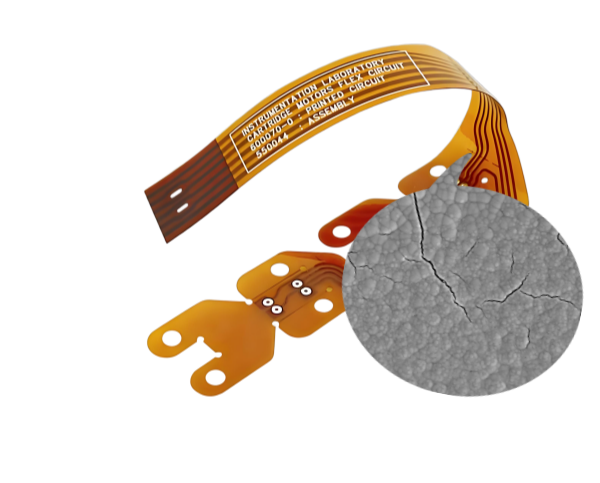
FPCs can get tired when bent many times. This can hurt how they work and last. Rigid boards do not get tired in this way and work more steadily.
Design and Manufacturing Difficulties
FPCs need a special design because they bend and stretch. This makes the design hard. Also, the making of FPCs needs very careful work. It is easy to get mistakes like short circuits or breaks in the lines.


