An Overview of Aluminum Substrates and Their Applications
 17 Apr 2025 16:22:37 GMT
PCBASAIL
What is Aluminum Substrate?
A circuit board made from aluminum core material is called an aluminum PCB. Due to its excellent heat dissipation capability, this type of PCB is commonly used in LED lighting products. The board has two sides: one side is white and is soldered to the LED pins, while the other side is in the form of aluminum. Typically, thermal paste is applied, and the contact is made at the thermal section.
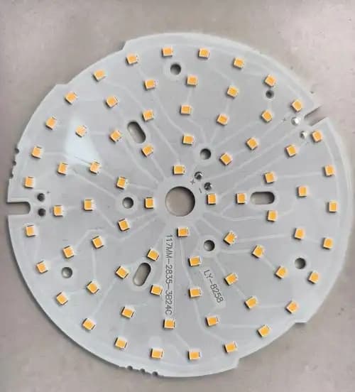
An aluminum substrate is a metal-based copper-clad laminate with good heat dissipation properties. Typically, a single-sided aluminum PCB consists of three layers: the circuit layer (copper foil), the insulating layer, and the metal base layer. It is also used for high-end applications designed as double-sided PCBs, with the structure being the circuit layer, insulating layer, aluminum base, insulating layer, and circuit layer. In rare cases, multi-layer boards can be made by combining conventional multi-layer boards with insulating layers and aluminum substrates.
Comparison Between Aluminum PCB and Copper Clad PCB & Overview of Aluminum PCB Applications in LED
LED aluminum substrates are PCBs, which are also known as printed circuit boards. The material of the circuit board is aluminum alloy. In the past, the common material for circuit boards was fiberglass. However, due to the high heat produced by LEDs, the circuit boards for LED lights are generally made from aluminum substrates that can quickly dissipate heat, while the circuit boards for other devices or electrical appliances still use fiberglass boards.
Compared to traditional FR-4, aluminum substrates can reduce thermal resistance to a very low level (thermal resistance is comprehensive) and reflect parameters that block heat transfer capability. In thermal engineering applications, sometimes heat transfer is enhanced by lowering thermal resistance, while in other cases, heat resistance is increased to suppress heat transfer. Aluminum substrates have excellent thermal conductivity, and their mechanical properties are superior to thick-film ceramic circuits.
The etched circuit layer (usually using electrolytic copper foil) is formed to create printed circuits for assembly and connection of components. Compared to traditional FR-4, the same thickness and line width allow aluminum PCBs to carry higher currents. This reduces product size, lowers hardware and assembly costs, and is suitable for SMT processes of power components.
However, aluminum PCBs cannot be used for PTH holes. In the 5G network era, radio frequency signals require good grounding performance, and heat dissipation requirements will be significantly higher. Aluminum substrates are not suitable for this, so copper-clad PCBs can be considered.
Copper Clad PCB
Copper-based printed circuit boards are among the most expensive metal substrates, with much better thermal conductivity than aluminum and iron-based substrates. They are suitable for high-frequency circuits, regions with high and low temperature fluctuations, as well as heat dissipation in precision communication equipment and the construction and decoration industries.
Generally, the surface finishes of copper-based circuit boards include gold immersion, silver plating, HAL, OSP, etc.
The circuit layer of copper-based PCBs requires a large current-carrying capacity, so thick copper foil should be used, generally ranging from 35μm to 280μm. The thermal insulation layer is the core technology of copper-based PCBs. The core thermal components are composed of a mixture of alumina, silicon powder, and epoxy resin. The heat resistance is low (0.15), with excellent viscoelasticity and thermal aging resistance, capable of withstanding mechanical and thermal stresses.
The metal base layer is the support component of copper-based PCBs and requires high thermal conductivity, usually copper-based PCBs, suitable for traditional mechanical drilling, punching, cutting, etc. The metal layer (block) mainly serves for heat dissipation, shielding, covering, or grounding. Due to the different properties of copper and aluminum, and the corresponding PCB processing capabilities, copper-based PCBs have more performance advantages than aluminum core PCBs.
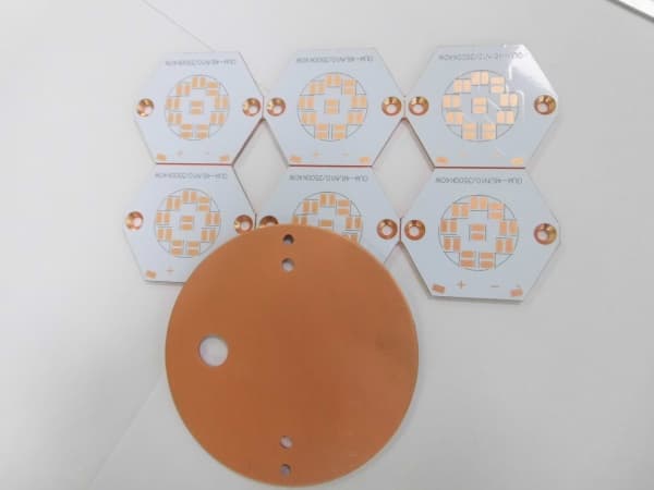
The thermal conductivity of copper is twice that of aluminum. The higher the thermal conductivity, the better the heat transfer efficiency and heat dissipation performance.
Copper-based PCBs can be processed into metallized holes, which is not possible with aluminum-based PCBs. Metallized mesh holes must be the same network, ensuring good signal grounding performance. Additionally, copper itself is weldable, completing the design's structural part. Installation is optional.
Copper substrates can have copper etched into fine patterns and processed into pad shapes, allowing components to be directly connected to pads for good grounding and heat dissipation.
Due to the different elastic moduli between copper and aluminum (the elastic modulus of copper is about 121,000 MPa, while aluminum's is 72,000 MPa), copper-based PCBs will have less warping and shrinkage compared to aluminum-based PCBs, resulting in better overall performance and stability.
Comparison Between Aluminum PCB and Copper Clad PCB & Overview of Aluminum PCB Applications in LED
Design Rules for Copper-Based Substrates:
Due to the thickness of copper, the minimum drilling radius must be 0.4 mm. The line width is determined by the thickness of the copper foil on the copper substrate. The thicker the copper foil, the wider the line. The minimum spacing must be larger.
Aluminum Substrate Pad and Wiring Design Specifications
1. Character and Graphic Requirements
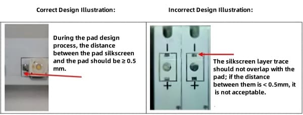
Characters, graphics, and other symbols should not be printed on the pads. The distance between the symbols and the edge of the pad should be greater than 0.5mm to avoid soldering defects due to ink contamination of the pad.
2. Requirements for Trace Routing and Shape
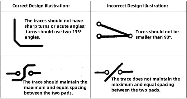
Trace Bending:
PCB Packaging: Single trace passing through pad treatment requirements.
3. Relationship Between Wiring, Current, and Temperature Rise
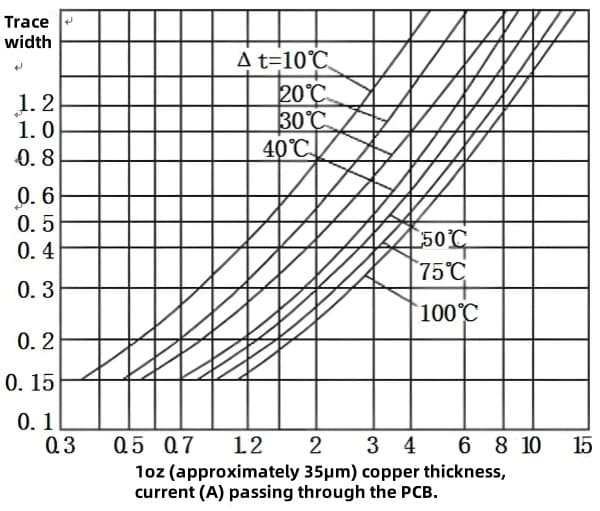
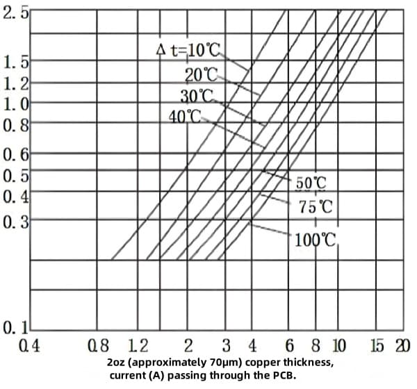
The current-carrying capacity of a trace depends on its width, thickness, and the allowable temperature rise.
The formula is I = KT(0.44)A(0.75), where K is the correction factor, for copper traces on aluminum substrates, K = 0.048; T is the maximum temperature rise (in °C); A is the copper cross-sectional area (in mils). Refer to the chart below for design guidelines.
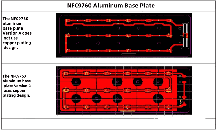
Impact of Copper Clad Design on Temperature Rise
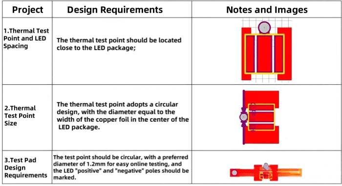
4. LED Test Point Design
Mark Point Design
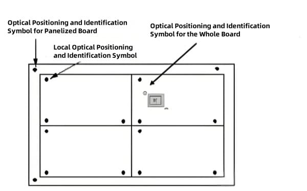
To improve the accuracy of surface mount component placement, correction marks (Marks) should be placed on the mounting layer. Mark points primarily include panel, whole board, and partial types (as shown below).
5. Mark Point Drawing (Single-Sided Board):
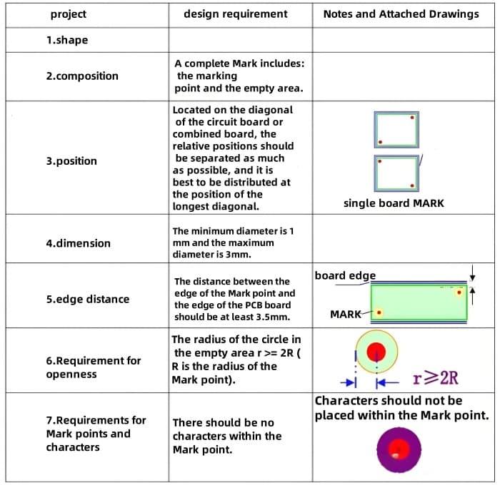
1.Top layer: Add solid pad (e.g., 1mm diameter)
Top solder mask: Add large solid pad (e.g., 3mm diameter) PCB manufacturers can identify it as a mark point.
2.Mark Point Design Requirements:
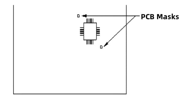
3.For aluminum-based substrates with IC chips and pin spacing less than 0.8mm, two marks should be added to the unit diagonal of the component as the correction marks for that component (as shown below).
6. V-Cut Design
General Principles:
V-Cut design is in the mechanical layer of the PCB.
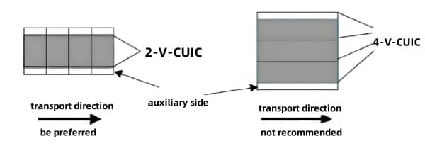
If the size of the PCB unit is smaller than 50x50mm, panelization is required.
The two sides of the PCB for transportation should leave a width of ≥3.5mm (138mil). No components or solder joints should be within 3.5mm of the edge on either side.
Edge trace width should be less than 0.5mm, and there should be a distance of more than 2mm from the V-Cut slot. If the edge trace width is greater than 1mm, this distance should not be less than 0.5mm to prevent traces from being scratched or severed during V-Cut.
7. Symbol Requirements
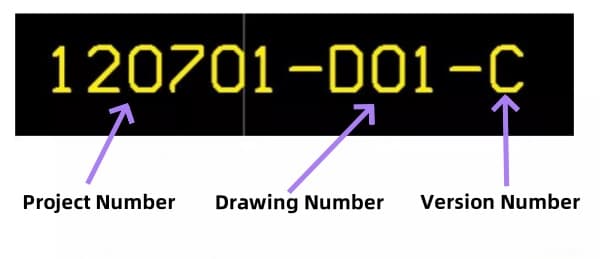
The silkscreen layer on the component side of the aluminum substrate must include the project number, drawing number, and version number (as shown below). The layout should be designed based on the actual size of the aluminum substrate, and the placement should be on the lower edge of the substrate. If a lens is used, the placement should avoid overlapping with the lens to ensure visibility of the symbols.
8. Trace Pad and LED Distance
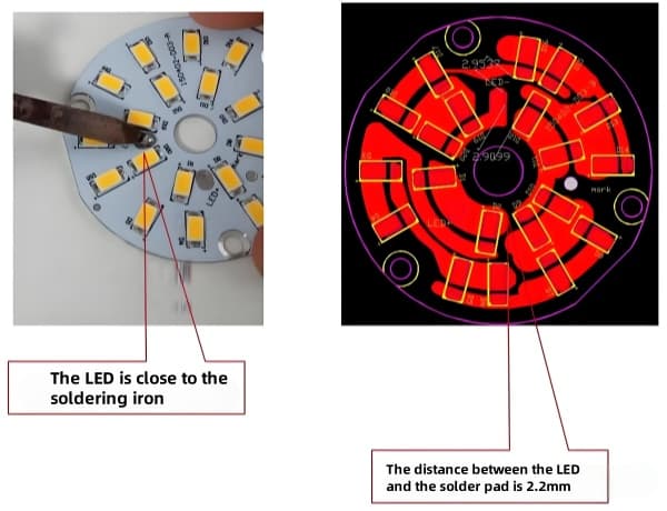
In actual production, when soldering the + and - traces of the driver to the aluminum substrate pads using a soldering iron, if the distance between the pad and the surrounding LEDs is too small, it can damage the LEDs or cause flux contamination, reducing LED life. Therefore, these two pads should maintain a minimum distance of 2.5mm from the surrounding LEDs.
