Table of Contents
What is LED PCB?
LED (Light Emitting Diode) is the abbreviation for light-emitting diode, a solid-state semiconductor device that directly converts electricity into light. Since its development, this semiconductor component has generally been used as an indicator light or display panel. However, with technological advancements, it can now be used as a light source. It not only efficiently converts electrical energy into light energy but also has a service life of up to tens of thousands to 100,000 hours. Additionally, it is non-fragile (unlike traditional bulbs), energy-saving, environmentally friendly (mercury-free), compact, applicable in low-temperature environments, directional in light emission, causes less light pollution, and offers a rich color gamut.

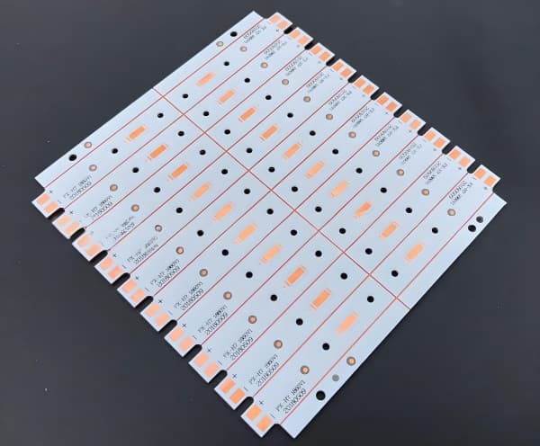
An LED PCB is a printed circuit board (PCB) to which LEDs are soldered, equipped with a chip that generates light through electrical connections. A heat sink and a ceramic base are used to connect the chip. Undoubtedly, the LED PCB is the core of LED lighting. Although an LED PCB tends to generate significant heat, traditional cooling methods are often inefficient. Metal-core PCBs are widely used in LED applications due to their strong heat dissipation capabilities, with aluminum being particularly common in manufacturing LED PCBs. Typically, an aluminum PCB includes a thin layer of thermally conductive dielectric material, which can transfer and dissipate heat much more efficiently than traditional rigid PCBs.
Advantages of LEDs
Lower Power Consumption: Replacing incandescent bulbs with LEDs can reduce power consumption by over 80%.
Longer Lifespan: LEDs typically have a service life of over 20,000 hours, lasting 24/7 for 3 years—25 times longer than incandescent bulbs. This not only saves costs but also reduces replacement frequency.
Higher Efficiency: Incandescent bulbs emit substantial heat, while LEDs can reduce this heat by up to 20%. This means using higher-power LEDs without unnecessary heat generation.
Smaller Size: Due to their compact design, LEDs come in various sizes and can be applied in diverse scenarios. Manufacturers can integrate LEDs into almost any product, from electronic devices and cars to traffic lights and road signs.
Environmental Friendliness: Unlike other bulbs, LEDs contain no mercury, making them less harmful to the environment and easier to dispose of.
Specific Manufacturing Processes for LED Packaging
Cleaning Process: Use ultrasonic cleaning for PCBs or LED brackets, followed by drying.
Mounting Process: Apply silver paste to the bottom electrode of the LED die, expand it, place the expanded die on a die-bonding stage, and use a die bond pen to mount each die onto the corresponding pad of the PCB or LED bracket under a microscope. Sintering is then performed to cure the silver paste.
Wire Bonding Process: Connect electrodes to the LED die using aluminum or gold wire bonders as current injection leads. Aluminum wire bonders are generally used when LEDs are directly mounted on PCBs.
Encapsulation Process: Protect the LED die and bond wires with epoxy resin through dispensing. The shape of the cured colloid on the PCB is strictly controlled, as it directly affects the light output brightness of the backlight product. This step also involves applying phosphor powder.
Soldering Process: If the backlight uses SMD-LEDs or other pre-packaged LEDs, solder the LEDs to the PCB before assembly.
Film Cutting Process: Use a punching machine to cut various diffusion films and reflective films required for the backlight.
Assembly Process: Manually install all backlight materials in their correct positions according to the design drawings.
Testing Process: Check the photoelectric parameters and light uniformity of the backlight.
Packaging Process: Package the finished products as required and store them in the warehouse.
Detailed Flow of LED Bead Packaging
LED Chip Inspection:
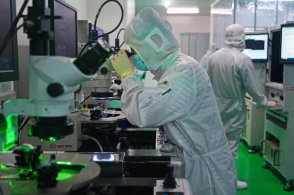
Microscopic inspection: Check for mechanical damage, pits, or cracks on the chip surface; verify that the size and dimensions of the LED chip electrodes meet process requirements; ensure the electrode pattern is complete.

Chip Expansion:
After dicing, LED chips are closely arranged with small spacing, making subsequent operations difficult. An expand machine is used to stretch the film adhering to the chips, increasing the spacing to approximately 0.6mm. Manual expansion is possible but prone to chip 掉落 (chip dropping) and waste.
Adhesive Dispensing:
Apply silver paste or insulating adhesive to the corresponding positions on the LED bracket. The key challenge is controlling the amount of adhesive, including its height and placement, as specified in the process. Silver paste and insulating adhesive have strict storage and usage requirements, such as aging, stirring, and shelf life.
Adhesive Preparation:
Contrary to dispensing, adhesive preparation uses a machine to apply silver paste to the back electrode of the LED first, then mounts the silver paste-coated LED onto the bracket. This method is more efficient than manual dispensing but is not suitable for all products.

Manual Die Placement:
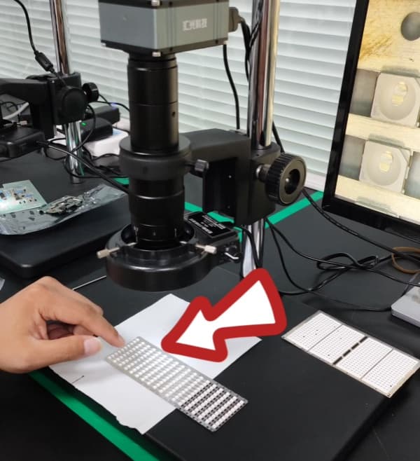
Place the expanded LED chips on a fixture of the die placement stage, position the LED bracket under the fixture, and use a needle to place each chip into the correct position under a microscope. Manual placement allows easy chip replacement, suitable for products requiring multiple chip types.
Automatic Die Mounting:
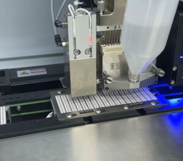
This process combines adhesive application and chip mounting: dispense silver paste on the LED bracket, use a vacuum nozzle to pick up the LED chip, move it to the target position, and mount it onto the bracket. Key steps include mastering equipment operation programming and adjusting adhesive application and mounting precision. Use 胶木吸嘴 (bakelite nozzles) to avoid damaging the chip surface, especially for blue and green chips, as steel nozzles can scratch the current diffusion layer.
Sintering:
Sintering cures the silver paste, requiring strict temperature control to prevent batch defects. Typical sintering conditions for silver paste are 150°C for 2 hours (or 170°C for 1 hour for adjustments). Insulating adhesive is sintered at 150°C for 1 hour. The sintering oven must be opened every 2 hours as per the process, with no unauthorized openings, and should not be used for other purposes to avoid contamination.
Wire Bonding:
This step connects the chip electrodes to external leads. There are two types: gold wire ball bonding and aluminum wire bonding. For aluminum wire bonding (as shown), the first bond is made on the chip electrode, the wire is pulled to the bracket, the second bond is made, and the wire is cut. Gold wire ball bonding involves forming a ball before the first bond. Key monitoring points include the shape of the wire arc, bond shape, and pull force. Factors affecting this process include wire material, ultrasonic power, bonding pressure, wedge selection, and wedge trajectory.
Dotting Encapsulation:
LED encapsulation methods include dotting, potting, and molding. Common challenges are bubbles, insufficient material, and black spots. Material selection (e.g., epoxy and bracket compatibility) is critical. Dotting is suitable for TOP-LED and Side-LED. Manual dotting requires high skill due to epoxy thickening during use, and white LED dotting may face color differences due to phosphor sedimentation.
Potting Encapsulation:
Used for Lamp-LEDs: inject liquid epoxy into a mold cavity, insert the bonded LED bracket, cure in an oven, and demold the formed LED.
Molding Encapsulation:
Place the bonded LED bracket into a mold, close the upper and lower molds with a hydraulic press and vacuumize, heat solid epoxy at the injection port, and press it into the mold channels with a hydraulic rod. The epoxy flows into each LED cavity and cures.
Curing and Post-Curing:
Curing: solidify the epoxy, typically at 135°C for 1 hour (molding encapsulation at 150°C for 4 minutes).
Post-curing: fully cure the epoxy and thermally age the LED, improving the bond strength between epoxy and bracket, usually at 120°C for 4 hours.
Trimming and Dicing:
Testing:
Packaging:
Electrostatic Discharge (ESD) Protection in LED Packaging
LEDs are semiconductor devices sensitive to static electricity, especially white, green, blue, and purple LEDs. Preventing and eliminating static electricity is crucial.
1. Main Causes of Static Electricity
Frictional Electrification: Static occurs when two different materials contact and separate. Insulative materials are more prone to this. Any two dissimilar materials can generate static when separated.
Inductive Electrification: For conductive materials, placing them in an electric field causes charge separation (like charges repel, opposite charges attract), resulting in surface charges.
Conduction: Charge transfer occurs when a conductive material comes into contact with a charged object, as electrons can move freely on its surface.
2. Hazards of Static Electricity to LEDs
Partial Damage: Instantaneous electric fields or currents generate heat, damaging the LED locally. Symptoms include increased leakage current, reduced brightness (color shift in white LEDs), and shortened lifespan.
Complete Failure: Electric fields or currents destroy the LED's insulation layer, causing permanent failure (dead lamp, no light emission).
3. ESD Mitigation Measures
Workstations & Equipment: Use anti-static workbenches and ground production equipment properly.
Facility Grounding: Install anti-static flooring in workshops and ensure proper grounding.
Personal Protective Equipment (PPE): Operators must wear anti-static clothing, wrist straps, gloves, or ankle straps.
Packaging Materials: Use anti-static packaging for products.
Ionization & Soldering: Employ ionizing blowers and ground soldering irons to eliminate static charges.

Applications of LED PCBs
LED PCBs offer excellent energy efficiency, low cost, and design flexibility, making them suitable for numerous lighting applications:
Telecommunications: LED indicators and displays are widely used in telecom equipment due to their heat dissipation capabilities. Aluminum-based PCBs play a key role here.
Automotive: Used in vehicle indicators, brake lights, headlights, etc. Aluminum PCBs are ideal for the automotive industry due to their durability and cost-effectiveness.
Computer Systems: LED displays and indicators are increasingly popular in computers. Aluminum PCBs are favored for their heat dissipation, also used in components like power supplies and CPU boards.
Medical Devices: High-power LED lights in surgical and diagnostic tools rely on aluminum PCBs for durability and heat management, ensuring consistent performance in healthcare settings. Aluminum PCBs are also used in medical scanning technologies.
 15 Apr 2025 16:36:31 GMT
PCBASAIL
