Flying‑Probe PCB Testing | Fast, Precise Electrical Check
 13 Jun 2025 17:12:39 GMT
PCBASAIL
Working Principle of Flying‑Probe Testing
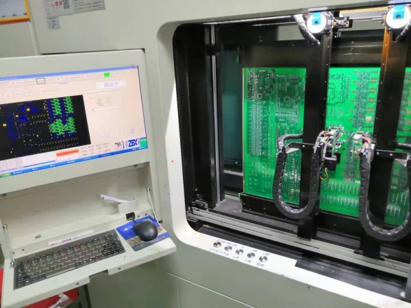
A flying‑probe tester is an enhancement over the traditional “bed‑of‑nails” high‑voltage automatic PCB tester, replacing the fixed needle beds with movable probes. During operation, the unit under test (UUT) is conveyed into the test apparatus via a conveyor belt or other transfer system. Test probes then make contact with each test pad and via on the PCB to examine individual components. Through a multiplexing system, each probe connects to signal drivers and sensors (such as power supplies, signal generators, digital multimeters, or frequency counters) to perform electrical tests on the UUT’s circuitry. While one component is being measured, the remaining circuits on the UUT are electrically shielded from interference by the probe fixture.
Flying‑probe testers are capable of detecting opens, shorts, and component‑value faults. A built‑in camera further assists by locating missing parts and verifying the correct orientation of polarized components (e.g., electrolytic capacitors).
With probe‑positioning accuracy and repeatability in the 5–15 µm range, flying‑probe systems can perform highly precise inspections. They eliminate many shortcomings of conventional PCB testing, such as lengthy 4–6 week test‑development cycles, high fixture costs for small batch runs, and the inability to economically or rapidly test prototype assemblies.

Key Testing Methods
Charge/Discharge‑Time (Net‑Value) Method
Each electrical network on a PCB has a characteristic charge/discharge time—its “net value.” If two nets share the same net value, they may be shorted.First board: Perform an all‑open (open‑circuit) test, then an all‑short test, and learn each net’s value.
Subsequent boards: Perform an all‑open test followed by a net‑value comparison; suspected shorts are then confirmed via resistance measurement.
Pros: Highly accurate and reliable results.
Cons: Long test time for the first board, multiple retests, and lower throughput.
Notable Example: The SPEEDY machine by MANIA.
Inductance Measurement Method
One or more large nets (usually ground planes) are excited as antennas; other nets inductively pick up this signal. By measuring each net’s inductance and comparing values, short circuits can be flagged for further resistance testing.Applicability: Effective for boards with ground or power planes; less reliable on two‑layer boards without such planes.
Pros: High reliability and fewer retests.
Cons: Reduced probe count available for measurements (since some probes deliver the excitation signal), leading to lower throughput.
Notable Example: ATG’s A2 and A3 systems—equipped with 8‑ and 16‑probe heads to boost efficiency.
Capacitance Measurement Method
Similar to the net‑value approach, this method relies on the capacitance between a conductor and a reference plane. CapacitanceC is given byεA/L, whereA is the conductor’s area andL its distance from the plane.Open circuits lead to reduced conductor area and lower capacitance.
Shorts increase the effective area and boost capacitance.
Workflow: Measure capacitance at each network’s endpoints during open‑circuit testing; discrepancies indicate opens and establish baseline values for short‑circuit comparisons.
Pros: Higher throughput.
Cons: More susceptible to environmental and geometric variations; lower reliability on networks with few endpoints.
Notable Vendors: HIOKI and NIDEC READ systems.
Phase‑Difference Method
A sine‑wave signal is injected into a ground or power plane; signal‑return layers detect the resulting phase lag, from which capacitance or inductance can be inferred.First board: Open‑circuit measurement, then phase values of other nets, followed by short‑circuit tests.
Subsequent boards: Open‑circuit check, phase‑difference scanning, and resistive verification of suspect shorts.
Pros: Good speed and reliability.
Cons: Suited mainly to multi‑layer (≥ 4) boards; two‑layer boards default back to resistance testing.
Example Supplier: MicroCraft.
Adaptive Testing Method
After each test step, the tester dynamically selects the optimal next method—net‑value, capacitance, resistance, or electric‑field measurement—based on the board’s characteristics and test criteria.Pros: Offers the fastest cycle times and highest test coverage.
Cons: Currently few commercial systems implement full adaptive logic.
Advantages of Flying‑Probe Testing
No Expensive Fixtures: Eliminates the $10 000–50 000 cost of custom bed‑of‑nails fixtures.
Rapid Prototyping: Shortens time‑to‑market by testing prototypes immediately, without waiting weeks for fixture design.
Low‑Volume Economics: Becomes cost‑effective even for small batch sizes.
Minimal Staffing: Reduces the need for highly experienced test‑development engineers.
Common Causes of Test‑Failure Flags
When a board fails open‑ or short‑circuit tests, the root causes typically fall into four categories:
Customer Data Files: The tester only compares against the provided netlist; missing or incorrect design data (e.g., omitted vias) lead to apparent failures.
Production Issues: Warpage, improper solder‑mask application, or inconsistent reference silkscreen can obstruct probe contact.
Data‑Conversion Errors: Using an outdated or incomplete engineering drawing for testing can omit critical features.
Equipment Factors: Hardware or software malfunctions in the tester itself.
In real production, post‑test assembly (SMT) sometimes uncovers via failures—boards may pass flying‑probe testing but still exhibit non‑conductive vias later. Common culprits include:
Drilling Residues: Epoxy‑glass dust left behind prevents proper copper plating; most flying‑probe tests will detect this, but sometimes it can slip through.
Copper Plating Defects: Insufficient plating time leaves vias underfilled; during soldering, incomplete copper dissolves, causing opens.
High‑Current Stress: Thick‑copper boards require advanced notice; excessive test currents can burn away thin via copper, mimicking a test‑escape.
SMT Soldering Errors: Excessive dwell time in the reflow oven melts via copper. Inexperienced operators may misjudge process parameters, resulting in via failures misattributed to testing errors.
Because most modern board shops can accommodate flying‑probe testing, choosing PCBASAIL—with our 100% flying‑probe coverage and advanced precision probing—is your ultimate safeguard against in‑field PCB failures.


