Poor Solderability in ENIG PCBs: Causes and Solutions
 11 Jun 2025 17:01:19 GMT
PCBASAIL
Abstract
The electroless nickel–electroless immersion gold (ENEIG) process has become the mainstream surface finish for lead‑free electronic products. Key factors affecting its solderability include the quality of the ENEIG plating, the cleanliness of the plated surface, and any nickel‑corrosion phenomena. This paper combines specific failure cases to detail the manifestations, analytical methods, and reasoning behind poor solderability of PCB pads caused by these factors, offering a reference for industry practitioners analyzing solderability issues.
1 Introduction
With the advent of the lead‑free era in electronics manufacturing, common PCB surface finishes now include electroless nickel–immersion gold (ENIG), immersion silver, immersion tin, and organic solderability preservative (OSP) films. ENIG — also called electroless nickel/gold, electroless nickel‑immersion gold, or chemical gold — applies a solderable coating onto bare copper on printed circuit boards (PCBs). It integrates solderability, contact conductivity, wire‑bonding support, and heat dissipation, meeting the increasingly complex requirements of PCB assembly and soldering, and is favored by PCBA (printed circuit board assembly) customers.
However, as the peak temperature for lead‑free reflow increases (with lead‑free solder melting at 217 °C), the process window narrows from 50 °C for tin‑lead soldering to just 15 °C for lead‑free soldering. The diversification of solder alloys, PCB surface finishes, and component surface treatments has introduced many compatibility challenges, particularly more complex solderability issues for ENIG‑finished PCBs. This paper focuses on several common failure cases of ENIG PCB solderability, summarizes their failure mechanisms and root causes, and provides robust analytical methods and approaches for resolving solderability issues.
2 Case Studies and Analytical Methods
2.1 Poor Solderability Due to Insufficient Gold Thickness
In ENIG, the gold layer thickness is typically controlled between 0.05 μm and 0.15 μm. If the gold layer is too thin, its protective effect on the underlying nickel diminishes. This becomes especially pronounced after long storage, pre‑placement baking, or high‑temperature aging during assembly, leading to noticeable solderability failures.
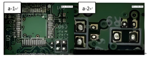
A case of soldering defects caused by insufficient gold thickness is shown in Figure 1, where the PCB pad appears white‑blanched and fails to wet with solder. X‑ray thickness measurements on unassembled pads (Table 1) revealed an average gold thickness of only 0.033 μm, below process requirements.
| Test Serial Number | 1 | 2 | 3 | 4 | 5 | Average | Customer Requirement |
|---|---|---|---|---|---|---|---|
| Gold Thickness (unit: μm) | 0.035 | 0.034 | 0.031 | 0.037 | 0.029 | 0.033 | ≥0.03 |
Scanning electron microscopy (SEM) and energy‑dispersive X‑ray spectroscopy (EDS) of the defective pads (Figure 2) showed no contamination, but a high oxygen content on the pad surface. This indicates that, due to the thin gold, nickel atoms migrated to the surface during reflow and oxidized to nickel oxide.

After acid‑etch cleaning and solder immersion of the defective pads (Figure 3), solderability was fully restored. The acid wash removed the nickel oxide layer, confirming that the original gold layer was too thin to protect the nickel during reflow, allowing formation of nickel oxides (melting point ~2000 °C) that blocked solder wetting.
2.2 Poor Solderability Due to Surface Contamination
2.2.1 Residual Ionic Impurities on Gold Surface
If halogen ions (chloride, bromide) or other acidic/alkaline residues remain after gold plating and are not thoroughly cleaned, they react with oxygen and moisture over time to oxidize the plating and reduce solderability. Even a clean board stored in humid or corrosive atmospheres can develop surface discoloration and solderability failures.
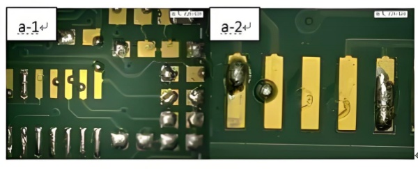
One example (Figure 4) shows pads with a “gold non‑wetting” appearance. SEM/EDS analysis of red‑discolored pads found elevated carbon levels, suggesting ionic contamination. After acid cleaning, solder immersion restored wetting, proving that a thin oxide layer formed by surface contaminants was the root cause.
2.2.2 Residual Solder‑mask Debris on Gold Surface
Other contaminants, such as solder‑mask residue, can also impair solderability. Figure 7 shows pads covered with green particulate contamination; solder paste would not wet these pads. SEM/EDS revealed that the contaminant’s morphology and elemental composition (Si, S, Ba) matched the solder mask, confirming solder‑mask residue.
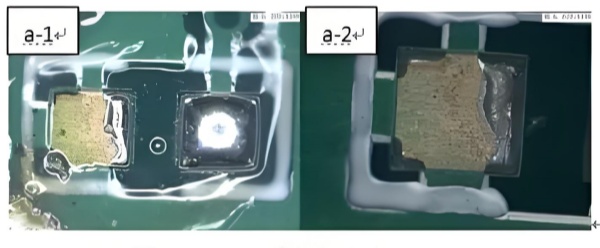
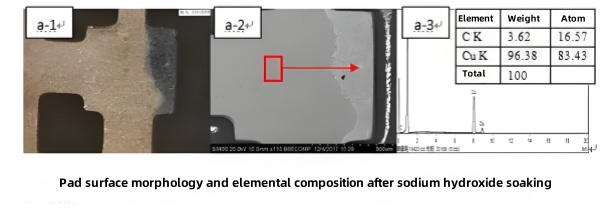
Removing the residue with 80 °C NaOH solution for 30 minutes (Figure 9) left a clean copper surface without Ni or Au. Subsequent solder immersion demonstrated good wetting, confirming that residual solder‑mask prevented proper ENIG deposition and solder diffusion.
2.3 Impact of Nickel Corrosion on Solderability
The nickel layer serves as a diffusion barrier between gold and copper and as the solderable base. Overly thin nickel weakens this barrier and thins the effective solderable layer. Because ENIG relies on a displacement reaction that forms a porous gold structure, nickel atoms can continue to be displaced under the gold if the reaction proceeds too far. Accumulated nickel ions beneath the gold oxidize to a black nickel oxide (“black pad”), which has very poor solder wetting.
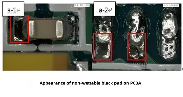
Figure 11
In one case (Figure 11), pads exhibited blackened areas after soldering. SEM/EDS of these pads showed elevated O, P, Ni, and Sn, and a cracked nickel lattice. Cross‑section microscopy (Figure 13) confirmed severe continuous nickel corrosion under the gold in both soldered and unsoldered pads, proving black‑pad formation was due to nickel corrosion.
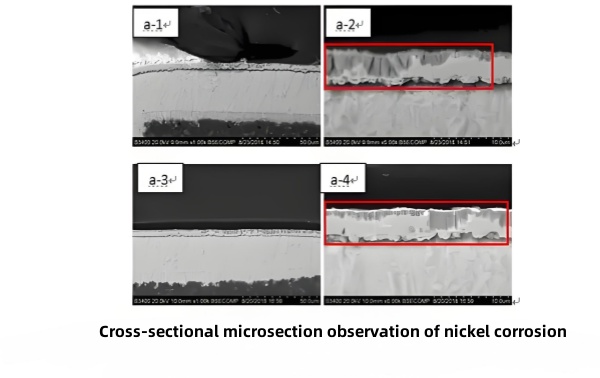
Figure 13
2.4 Poor Solderability Due to Damage in Gold or Nickel Layers
Gold provides corrosion and oxidation protection; any scratches, pores, or sand‑blasted damage compromise that protection. The nickel layer beneath then oxidizes, preventing proper solder wetting.
2.4.1 Pores in the Gold Layer
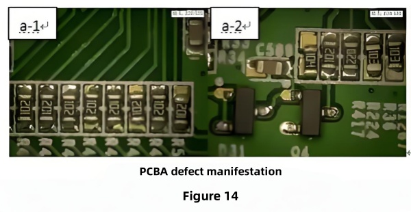
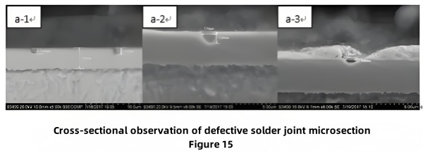
Figure 14 shows pads with numerous pores. SEM/EDS detected C, O, P, Ni, Sn, and Au; nickel content was ~50%, and linear scans showed gold thickness dropping to zero at pores. Cross‑section images (Figure 16) measured pore widths of 1.46–1.71 μm and depths of 0.45–1.29 μm, where soldering was discontinuous. These defects stem from inherent pores in the nickel layer that gold could not fill, leading to nickel oxidation.
2.4.2 Scratches on the Gold Surface
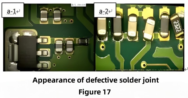
Figure 17 reveals dense scratches exposing nickel. SEM/EDS confirmed high C and O at scratched areas. After cleaning with isopropanol, soldering still failed; after acid cleaning, wetting was restored, showing that scratches exposed nickel which oxidized under air.
2.4.3 Sand‑blasted Gold Surface
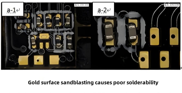
Figure 20 depicts sand‑blasted gold pads. SEM/EDS showed abnormal morphology consistent with sand‑blasting damage: a thinned gold layer exposing nickel, which then oxidized. No other contaminants were found.
3 Conclusions
Main failure causes in ENIG solderability include insufficient plating thickness, surface contamination, nickel corrosion (black pad), and damage to the gold or nickel layers.
During reflow, the plating’s primary role is to protect the solderable surface from oxidation and contamination, enabling rapid fusion of solder and substrate to form reliable joints. Because the nickel layer acts as the diffusion barrier and base for soldering, any thinning or damage of the gold layer, or intrinsic defects in the nickel, poses a risk of insufficient protection and consequent solderability failure.


