Complete PCB Process Guide for Hardware Engineers
 04 Jun 2025 11:28:05 GMT
PCBASAIL
The Structure of Multi-Layer PCB
Multilayer PCBs are mainly composed of glass fiber boards and copper circuits stacked together. Asking the following questions can give you a deeper understanding of PCB boards:
PCB Circuit
How to Make Circuit?
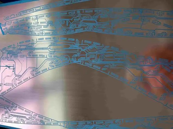
The original PCB substrate is a thin glass fiber board covered with copper foil on both sides, a complete piece of copper foil. The circuit is engraved on the copper foil. Similar to developing photos, Gerber has images of each layer, and the image is made into a negative film (film). When light is projected onto the substrate, the substrate will show the pattern on the film. The actual work is to corrode the copper in the unnecessary area through chemical etching, and the remaining is the circuit. Both sides are the same. For a two-layer board, you only need to make the circuit of the substrate.

Note: The glass fiber board here is helpful for understanding. In fact, there are other resin materials in it, and the commonly used model is FR-4.
How to Make Multiple Layers?
Take a solid piece of plastic and want to embed some metal in it. What should I do? It is impossible to install metal inside without any damage. But we can use two pieces of plastic to clamp a piece of metal, and the metal will go inside the solid plastic. This is the origin of the inner layer circuit of the multi-layer circuit board: stacking up layer by layer.
First make the circuit of the two-layer board, and then press a single-sided copper foil substrate on the upper and lower sides of the substrate, and you will have 4 layers. The method of the surface circuit is exactly the same as the circuit of the substrate. If you want to make 6 layers, press two more layers of substrate. Press more if you want more.
Usually the substrate in the middle will be thicker, and the substrates on both sides will be much thinner. Most circuit boards will not make the thickness of each layer uniform.
How to Make a Hole?
The two sides of the substrate are not connected. In order to connect the circuits on both sides, you need to drill a hole. However, there is only a hole, and the air in the hole still cannot conduct electricity. At this time, you need to electroplate in the hole. After plating a layer of copper, the circuits on both sides can be connected through the copper in the hole.
The principle is very simple, but the actual process is very complicated. It is necessary to cover the circuit and do surface treatment in the hole before copper can be plated.
How to Drill Holes
Remember that we will output the drilling diagram in Gerber? The drilling diagram marks the relative coordinates of each hole and inputs it into the machine tool. The manipulator uses a thin drill bit to drill holes one by one on the circuit board. This is a mechanical hole. The minimum diameter of commonly used mechanical holes is 0.2mm, and there are also 0.25 and 0.3mm. Think about it, a drill bit with a diameter of 0.2mm is only a little thicker than a hair, and it is easy to bend or break. This is why almost no factory is willing to make 0.15mm mechanical holes, and a circuit board with a hole of 0.2mm will also be more expensive than a circuit board with a hole of 0.25mm. This hole that passes through the entire circuit board is called a "through hole". A hole that has been opened. If the two sides of the through hole are not covered with paint, you can see that the middle is empty with the naked eye. If you solder, you will find that solder has leaked to the opposite side.

For HDI boards (High Density Interconnector), there is also a special hole, the laser hole. The laser ablates the circuit board and burns a hole. The laser will not break, and the beam can be made very thin. Laser holes with a diameter of 0.1mm are usually used on circuit boards. The laser ablates the material through high temperature. The main components of the substrate are glass fiber and resin, and the melting point is not high, so it is easy to burn through with the laser. But when the laser encounters copper foil, it cannot be burned through. Therefore, only one side of the laser hole is open, and the other side will be sealed by the copper foil and cannot be seen through. Therefore, it is called a blind hole.
For the inner layer circuit, you can first drill the hole and then press the outer layer circuit. At this time, the original through hole is buried in the board, so it is called a buried hole. It is essentially a through hole.
Can you only drill half and leave half?
For example, only 1-2 layers of the circuit board are drilled, and 3-4 layers are retained. I'm sorry, the processing difficulty is too great, and the depth cannot be so precise. Therefore, the openings on the circuit board, as long as they are mechanically opened, must be punched through, and the depth cannot be limited. If you have to do it, there are also some special processes, such as drilling holes in the substrate in advance. Such processes are not common, so the price is also very high.
How Wide is the Line Drawing?
The unit of the line on the PCB board is mil. Mil = one thousandth of an inch. 0.0254 mm. In layman's terms, it is 4mil = 0.1mm.
The current mainstream line width and line spacing in China are generally 4mil. It is 0.1mm. If the width is too narrow, it will be difficult to process. As mentioned earlier, the wire is etched on the copper foil through a photo. If the line is too narrow, it is easy to corrode and break. If the line spacing is too narrow, it is easy to corrode and cause a short circuit. On the current mainstream multi-layer HDI board, the line width and line spacing can be 2.5mil locally and 3mil overall. If the line is thin, the defect rate will be higher and the unit price will be more expensive.
Since the price will rise if the line is too thin, can we make the line thicker? No, if the line is too thick, the difficulty of PCB drawing will increase. And the line thickness is closely related to the signal type. The line width and line spacing must be reasonably selected according to the type and parameters of the signal transmitted on the circuit. PCB draftsmen are also required to be familiar with the principle design. For example: the width of the power line should be designed according to the maximum current passing through, usually calculated as 40mil passing 1A current. 4mil is enough for ordinary signal lines. RF lines need impedance matching, and the line width should be calculated according to the board and the number of layers. When drawing the schematic diagram, the line name should also be clearly marked, so that the PCB draftsman can easily and accurately see the function of this line from the name, and then take the appropriate routing method.
Can the Via be Made Casually?
Yes, but no.
Let's talk about "yes" first. Just like stairs, there can be stairs from the first floor to the second floor, from the second floor to the third floor, and from the third floor to the fourth floor. So can we just build a ladder and go from the first floor to the third floor, or directly from the first floor to the fourth floor? Theoretically, yes, this is called an arbitrary layer interconnection board. You can connect from any layer to any other layer. Take the 8-layer arbitrary interconnection as an example. You can directly connect from 1 to 8, or from 1 to 2 to 7, or from 2 to 3 to 8, or from 4 to 5 to 8. You can draw whatever you want, and you can run the lines however you want. There is almost no situation where the lines cannot be connected. Just thinking about it makes you happy, right? But this circuit board has only one disadvantage: it is expensive. It is extremely expensive. It is an order of magnitude more expensive than ordinary circuit boards! In the field of consumer electronics, only models like iPhone that are not short of money are willing to do this. Other models, whether Huawei mobile phones or OPPO vivo, do not have such mass-produced models.
Because it is expensive, it is "not possible". Circuit boards used in the fields of smart hardware and the Internet of Things are generally not wasted. When the performance is met, try to use simple processes to achieve it, which can effectively reduce costs.
The lowest cost is the through-hole board. After pressing, drilling a hole once, and copper plating once, it is completed. There are many fewer processes, saving time and cost.
Let's talk about the concept of first-order and second-order.
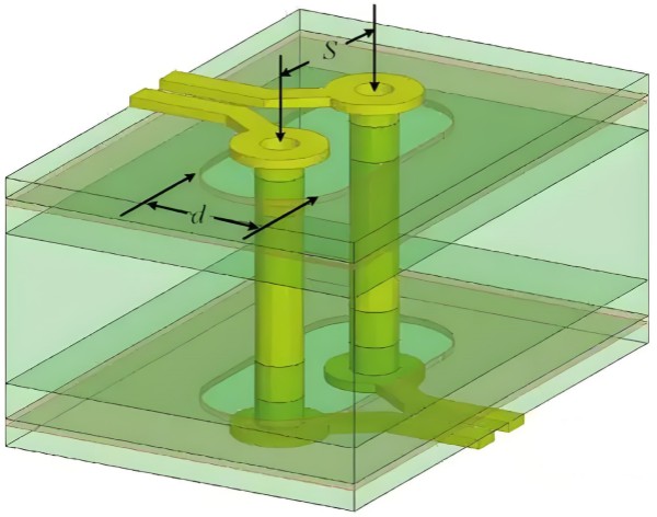
As shown in this picture, it is the most traditional second-order non-overlapping stacking structure. Through holes and buried holes are mechanical holes, and blind holes are laser holes. It looks like there are two steps, so it is called second-order. It can also be understood that there are several layers of laser holes, which is the number of steps of the board. Overlapping holes, as the name suggests, is to overlap the holes together. Usually, the holes are staggered, that is, one hole is not punched on top of another hole, also known as "staggered holes". But laser holes can be stacked together to form stacked holes. Laser holes and mechanical holes cannot be stacked together. When designing PCBs, staggered holes are manifested as 1-2 and 2-3 laser holes. Overlapping holes are manifested as 1-3 layers of laser holes.
The principle of laser holes was discussed earlier. The laser energy is limited, and it can only penetrate relatively thin plates, and it needs to hit the copper foil before it can stop. Because the middle of the mechanical hole is hollow, if a laser hole is punched on the mechanical hole, the laser will pass through. The reason why two laser holes can be stacked is not that the inside of the laser hole is not hollow, but that the inside of the inner laser hole is blocked with copper through the "electroplating filling" process, and then the surface is smoothed. For the outer laser hole, the inner laser hole looks like a piece of copper foil, not a hole. So why can't the inner hole be electroplated and filled? The inner diameter of the inner mechanical hole is too thick, and the copper plating cannot be so thick and cannot be filled.
Originally, a circuit board with only one through hole needs one more punching and electroplating process to make a first-order board, and one more punching and electroplating process to make a second-order board. If a stacked hole is made, an electroplating filling process is required. The more processes, the higher the cost, the higher the processing complexity, and the lower the yield.
Gold Plating Layer
The circuits on the PCB are all made of copper foil. The oxidation resistance of pure copper is not strong. It will oxidize quickly when directly exposed to the air. Therefore, the exposed pads of the circuit board need to be treated, which can not only prevent the oxidation of the copper pads, but also improve the solderability.
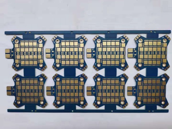
There are three colors of pads on circuit boards that we usually see, gold, silver, and orange-red. They are immersion gold, tin spraying, and OSP. Immersion gold is to deposit a layer of nickel gold on the surface of the pad by chemical methods. Tin spraying is to spray a layer of tin on the surface of the pad. OSP is an inorganic film. All three methods are used to improve solderability. Immersion gold has the best corrosion resistance, followed by tin spraying, and OSP is the worst.

On large-sized low-cost circuit boards, tin spraying is more commonly used.
On small-sized precision circuit boards, such as mobile phones, smart hardware, etc., immersion gold is still the main process.
OSP can be understood as a protective film covering copper, which makes the inner copper less easily oxidized, and can automatically melt and act as a flux during welding. Because it does not contain gold, the price of OSP is slightly lower than immersion gold. Usually on circuit boards, pads that need to be exposed to the outside for a long time, such as ground pads, need to be treated with immersion gold, and pads that need to be welded can be treated with OSP.
Because the coating of the circuit board is not absolutely anti-oxidation, the circuit board has a shelf life. If it is stored in the air, the immersion gold board is about half a year, and the OSP board is no more than one month. If it is vacuum-sealed, the immersion gold board can be used for one year, and the OSP board can be used for several months. For an expired motherboard, the pass rate may drop a lot when the solder pad is oxidized during patching.
Price Trend
Engineers are often insensitive to product prices, which is wrong. Hardware engineers must always have the awareness of "saving money" and save as much as possible while ensuring performance and cycle. For example, if a product saves 1 yuan and sells 1 million units, it can save 1 million.
The price of PCB = board + many films + many processes + labor costs + scrapped boards. The board and labor costs are not much different, and the price difference is mainly reflected in the process and scrap rate. The high scrap rate of the process naturally makes the cost more expensive.
The more layers, the more expensive it is. For every 2 layers added, the price will increase by about 30%.
The more levels, the more expensive it is. For every additional level, the price will increase by about 30%.
The price will also increase if special processes are used. Overlapping holes, mechanical holes with a diameter of 0.2mm, and line widths and line spacings less than 3mil will each cause a 10-20% price increase.
This price increase is calculated by multiplying each item, not by adding each item. It can be understood that for every additional complex process, the board factory's yield will decrease a little. With ten processes added, the total yield is the product of ten times the yield. That's why any layer of interconnected circuit boards is ridiculously expensive.


