Pin Grid Array (PGA) vs Ball Grid Array (BGA) Guide
 22 May 2025 15:33:50 GMT
PCBASAIL
PGA Packaging (Pin Grid Array)
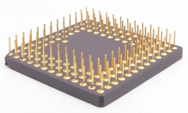
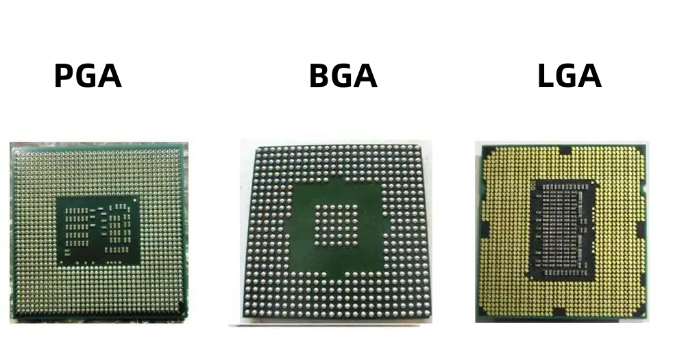
Chips packaged with this technology feature multiple square arrays of pins both inside and outside. Each square array of pins is arranged at specific intervals along the chip's perimeter, forming 2 to 5 concentric circles depending on the number of pins. During installation, the chip is inserted into a specialized PGA socket.

Pin Grid
The Pin Grid Array (PGA) packaging technology (Ceramic Pin Grid Array Package) involves chips with multiple square pin arrays inside and outside. These pin arrays are spaced at fixed intervals along the chip's perimeter, forming 2 to 5 circles based on the pin count. Installation requires inserting the chip into a dedicated PGA socket. To facilitate easier CPU installation and removal, starting from the 486 chip, a ZIF (Zero Insertion Force) CPU socket was developed specifically for PGA-packaged CPUs, meeting the requirements for quick and safe insertion/removal. This technology is typically applied in scenarios requiring frequent plugging and unplugging.
Array Pins
PGA (Pin Grid Array) is a plug-in packaging type with vertical pins arranged in an array on the bottom surface, each approximately 3.4mm long. Surface-mount PGA variants have arrayed pins on the bottom with lengths ranging from 1.5mm to 2.0mm. A schematic diagram of PGA packaging is shown below. Most are ceramic PGAs, used for high-speed large-scale logic LSI circuits, with higher costs. The pin center pitch is typically 2.54mm, and the number of pins ranges from 64 to around 447. To reduce costs, the packaging substrate can be replaced with a glass-epoxy printed circuit board. There are also plastic PGAs with 64 to 256 pins.
Additionally, there is a short-pin surface-mount PGA (bump-bonded PGA) with a pin center pitch of 1.27mm. Mounting is achieved via bump bonding to the printed circuit board, hence the name "bump-bonded PGA." With a pin pitch half that of plug-in PGAs (1.27mm), the package body can be smaller while accommodating more pins (250–528), making it suitable for large-scale logic LSI packaging. Substrate materials include multi-layer ceramic and glass-epoxy printed circuit boards, with multi-layer ceramic substrates already in practical use.
Common Models
BGA Packaging (Ball Grid Array)
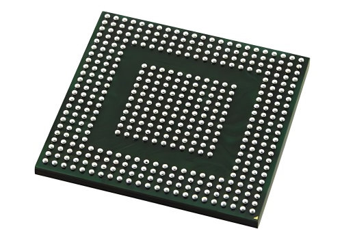
BGA, short for Ball Grid Array, forms an array of solder balls on the bottom of the package substrate as I/O terminals for interconnection with a printed circuit board (PCB). Devices using this technology are surface-mount components.

Introduction to BGA
In today’s information age, with the rapid development of the electronics industry, products such as computers and mobile phones have become increasingly popular. Consumers demand more functions, higher performance, smaller size, and lighter weight from electronic products. This drives the electronics industry toward multi-functionality, high performance, miniaturization, and lightness. To achieve this, IC chips require smaller feature sizes and higher complexity, leading to more I/O pins and higher packaging density. To meet these demands, advanced high-density packaging technologies like BGA have emerged.
BGA packaging originated in the early 1990s and has matured into a high-density packaging technology. Among all semiconductor IC packaging types, BGA grew the fastest between 1996 and 2001, with production reaching approximately 1 billion units in 1999. Currently, this technology is primarily used for high-density, high-performance devices and continues to evolve toward finer pitch and higher I/O counts. BGA is suitable for packaging PC chipsets, microprocessors/controllers, ASICs, gate arrays, memories, DSPs, PDAs, PLDs, and other devices.
Structural Characteristics
BGA components are mainly classified by packaging material:
PBGA (Plastic Ball Grid Array)
PBGA uses a BT resin/glass laminate as the substrate and plastic (epoxy molding compound) as the sealing material. Solder balls can be leaded (63Sn37Pb, 62Sn36Pb2Ag) or lead-free (Sn96.5Ag3Cu0.5), and no additional solder is required to connect the solder balls to the package.
Some PBGA packages have a cavity structure, either cavity-up or cavity-down. These cavity PBGA packages are designed to enhance heat dissipation and are called thermal-enhanced BGA (EBGA) or CPBGA (Cavity Plastic Ball Grid Array).
Advantages of PBGA:
Disadvantages of PBGA:
CBGA (Ceramic Ball Grid Array)
CBGA has the longest history in the BGA packaging family. Its substrate is multi-layer ceramic, with a metal cover welded to the substrate using sealing solder to protect the chip, leads, and pads. Solder balls are made of high-temperature eutectic solder (10Sn90Pb), and low-temperature eutectic solder (63Sn37Pb) is used to connect the solder balls to the package.
Advantages of CBGA:
TBGA (Tape Ball Grid Array)
TBGA has a cavity structure, with two chip-to-substrate interconnection methods: flip-chip bonding and wire bonding. The chip is flip-chip bonded to a multi-layer flexible tape substrate, with peripheral array solder balls (as I/O terminals) mounted under the tape. Its thick sealing cover also serves as a heat sink, reinforcing the package and ensuring good coplanarity of the solder balls under the flexible substrate. The chip is bonded to a copper heat sink in the cavity, with interconnections between chip pads and tape substrate pads achieved via bonding wires. The chip, wires, and tape pads are encapsulated (potted or coated) with a sealant.
Advantages of TBGA:
Other BGA Packaging Types


