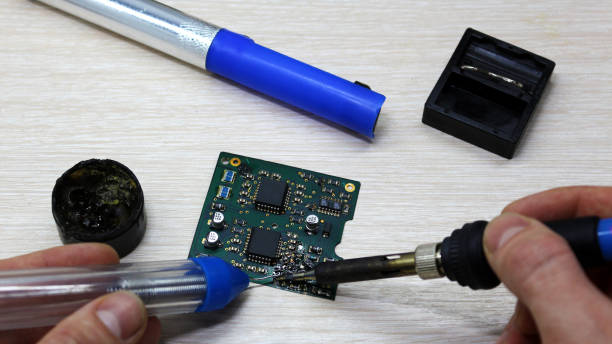
What are dry solder joints and solder beads?
 20 May 2025 14:48:11 GMT
PCBASAIL
During the PCB (printed circuit board) assembly process, dry solder joints and solder beads are very common welding defects, which may cause circuit malfunction or even failure. Let's take a deeper look at what dry solder joints and solder beads are and common problem solutions.
1. Dry Solder Joint
1.1 Definition
Dry solder joints refer to the failure to form a reliable metallurgical bond between the solder (tin paste) and the component pins and pads. The surface appears to be welded, but the actual electrical connection is unstable or the mechanical strength is insufficient.

1.2 Main Reasons
1.3 Solutions
(1) Clean the surface to remove contaminants. Wipe the component pins and PCB pads with anhydrous alcohol or flux cleaning agent to remove oxides, grease, flux residue or dust.
(2) For severely oxidized copper feet, we can first dip a small amount of solder and flux into the soldering iron for tinning to form a new solder surface.
(3) To control the quality, use Automatic Optical Inspection (AOI) after reflow to identify abnormal solder joints (insufficient solder, irregular contours).
(4) Use X-ray Inspection (AXI) to find solder joints (such as BGA) and observe the connection status between solder balls and pads.
(5) Perform functional tests on PCBs, test working environment vibration and repeatedly switch temperature tests to expose potential dry solder joints.
2. Solder Beading
2.1 Definition
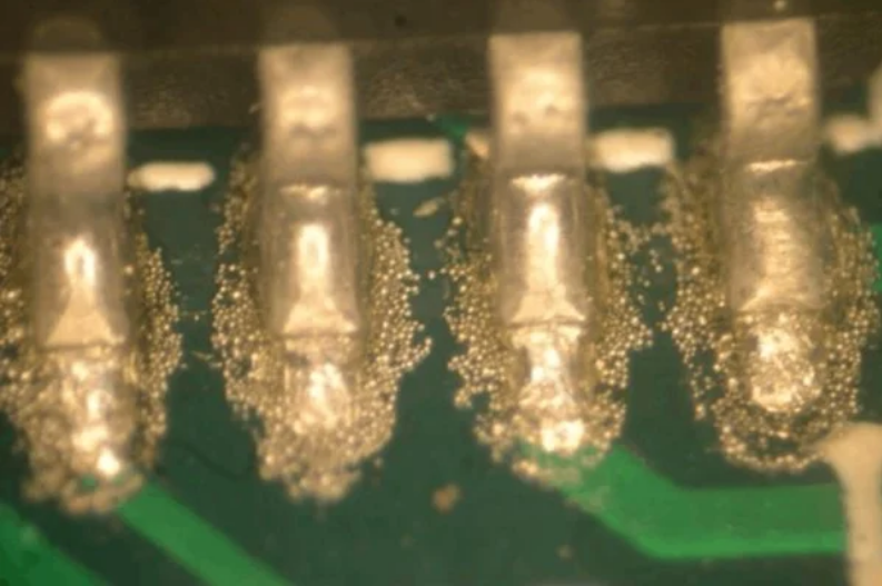
After soldering, the solder is spherical (usually 0.1-0.3mm in diameter) or irregular, with a smooth surface or burrs, which may cause short circuits or contamination. It mainly appears around the pad, the gap between component pins, the gap between PCB solder mask or large copper foil areas. During reflow soldering, tin beads may splash on the surface of the IC package.

2.2 Main Reasons
(1) Excessive solder paste printing, too large stencil opening size, or too thick stencil thickness will lead to excessive accumulation of solder paste. After heating, part of the solder will break away from the solder joint due to gravity or tension to form solder beads.
(2) Moisture in the solder paste causes the solvent inside to volatilize rapidly when heated during soldering, pushing the molten solder to splash and form solder beads.
(3) If the Sn content in lead-free solder paste is too high, the surface tension during melting will be low, making it prone to forming small spherical particles.
2.3 Detection Methods
(1) Visual inspection (VI): Observe the PCB surface through a magnifying glass or microscope to see if there are tiny spherical particles.
(2) Automatic optical inspection (AOI): High-density circuit boards can use image recognition technology to identify tin beads.
(3) Ion contamination test: Through the ionic contamination of the PCB surface and measuring the electrical inversion rate, the risk of tin beads containing metal ions can be indirectly determined.
3. The Difference Between Cold Solder Joint and Solder Bead
4. Summary
In short, dry solder joint and solder bead are defects that need to be avoided in PCB assembly. Dry solder joint is mainly caused by substandard welding process, and solder bead is mainly related to solder control and environmental parameters. By optimizing design (such as increasing pad spacing), strictly implementing process standards (such as temperature and curve monitoring) and introducing automated detection (such as AOI optical detection), the incidence of two types of defects can be significantly reduced and product reliability can be improved.
Solder bead may cause instantaneous short circuit or long-term leakage, get stuck in the gap of components during thermal expansion and contraction, causing mechanical failure and accelerating PCB aging.
To Meet Your Needs, You Need a PCB Company with the Following Qualities:
Are you looking for a PCB assembly supplier? You can provide information such as the number of board layers, component types, and demand.
PCBASAIL is your reliable supplier.


