Effects and Selection of PCB Panelization Methods
 28 Apr 2025 14:35:30 GMT
PCBASAIL
What are the effects of different PCB panelization methods?
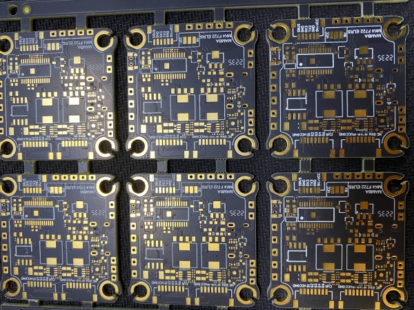
In the design and production process of PCB, the panelization method can directly affect production efficiency, cost and finished product quality. Panelization combines multiple independent PCB units into a large board, which can not only improve the utilization rate of the board, but also optimize the efficiency of SMT patch, testing and transportation. However, panelization must take into account the connection method between the boards. There are three common types of panelization: V-cut, stamp hole and hollow connecting strip. V-cut is more commonly used for regular boards. You only need to put two boards together and leave a V-cut gap between the boards. Snap offhole are more commonly used in special-shaped boards, and multiple holes are punched at the connection of the boards. Hollow connecting strips use very narrow boards for connection, which are more commonly used in boards with half-hole processes.

Why we need panelization?
1) Improve efficiency and reduce costs
When producing a single small-size PCB (such as a 10*10mm sensor board), the direct processing efficiency is very low. After panelization it will form a standard size (such as 300*250mm), the equipment processing area can be fully utilized and the machine change time can be reduced. It can also optimize the utilization rate of materials. By reasonably arranging the unit boards (such as yin-yang assembly and rotational symmetry assembly), the utilization rate of PCB boards can be increased from 60% to more than 90%, significantly reducing costs. And the panelization can also reduce the development cost of jigs and welding carriers.
2) Ensure process stability
After panelization, when we assemble, the nozzle of the SMD machine can continuously mount multiple units on the panel, reducing the frequency of nozzle movement and increasing the speed by 30%-50%. Usually, a 5mm process edge is reserved on the edge of the panel. During wave soldering, it is convenient for mechanical clamping and furnace passing, and can prevent the small board from being deformed or falling due to welding due to its small size. If a thin PCB (such as 0.4mm thickness) is produced, the overall strength will be improved after panelization, and it is not easy to bend or scratch.
3) Quality control
Panelization can also integrate test coupons or auxiliary positioning holes, and support flying-probe testing, AOI and other inspection equipment to complete multi-board testing at one time. All PCBs in the same panel undergo the same manufacturing conditions, such as etching, drilling and copper plating, which can reduce batch differences and ensure the high quality of the board.
4) Adapt to complex designs and special needs
PCB production is not just about regular shapes. When producing irregular PCBs such as round and L-shaped, we choose panelization to fill in blank areas to avoid waste in cutting panels. When producing PCBs in the field of communication modules, the main control board, RF board, and power board can be combined to achieve "one-time assembly, whole board testing". Panelization can contain different types of PCBs to meet the delivery of small batch and multi-variety orders.
How are the three common panelization methods made?
The choice of panelization method directly affects the efficiency, feasibility and cost of PCB manufacturing. The current mainstream panelization methods include V-cuts 、Snap off hole and Tab Routing.
1. V-cut
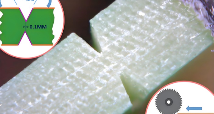
V-cut panelization is to cut a V-shaped groove at the connection of two boards by a mechanical rotating blade, leaving a connection part of about 1/3 of the board thickness, so the board at this place is relatively thin and easy to break. This method is fast in splitting boards and has high edge flatness. It is suitable for circuit boards with straight edges such as rectangles or squares, but cannot be used for curved board splitting because too deep a cut can easily cause burrs on the edges after splitting. It is typically used in standardized rectangular PCBs such as consumer electronics motherboards and power modules.

2. Snap off hole
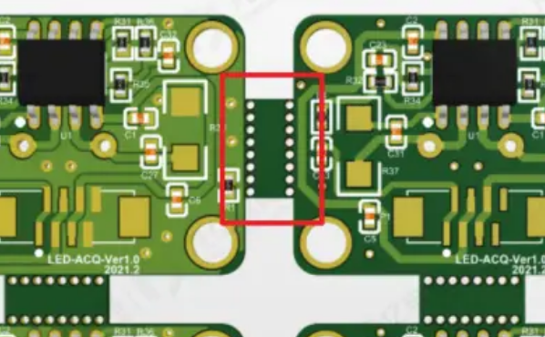
Snap off hole are another way to connect PCBs, and are generally used more in irregular boards. This panelization method connects the edges of two boards through a small piece of board. There are many small holes at the connection between this small board and the two circuit boards, usually with a hole diameter of 0.6-1.0mm. The edge of the board after breaking is like the edge of a stamp, so it is called a snap off hole. This type of panelization supports heterogeneous boards, circular, polygonal, etc., and the direction of panel separation is flexible. However, the serrations on the edges after panel separation are more obvious, requiring secondary grinding, and the connection strength of the stamp hole panelization is low, and it is easy to break accidentally during transportation. It is typically used in heterogeneous PCBs such as LED boards and wearable device boards.

3. Tab Routing
The Tab Routing method is similar to the stamp hole, the difference is that the connecting part of the connecting strip is narrower and there are no holes on both sides. However, when the Tab Routing panel is separated, a milling cutter is used to cut and separate the board. After the board is separated, there will be a more obvious convex point. The stamp hole panel will also have a convex point, but because it is separated by vias, it is not so obvious. So why do we still use the Tab Routing method to assemble the board? Because when the board design is surrounded by half-hole modules, stamp holes and V cuts cannot be used, and can only be connected at the four corners of the module through hollow connecting strips. The Tab Routing has high panel separation accuracy of ±0.1mm, no burrs on the edges, and is suitable for precision assembly. However, the processing of hollow connecting strips takes a long time and the cost is higher than V-CUT and stamp holes. It is typically used in medical equipment PCBs, high-frequency radio frequency boards and other fields with high dimensional accuracy requirements.
How to choose the right panelization?
Simple comparison of three types of paneling:
V-cut | Snap off hole | Tab Routing | |
Cost | Low | Medium | hign |
Efficiency | High(Auto) | Low(manual) | Medium(Using equipment) |
Edge quality | Good (needs slight polishing) | General (need to deburr) | Excellent (immediately available) |
Applicable thickness | 0.6-3.0mm | 0.4-4.0mm | 0.2-2.0mm |
IPC Standard | IPC-2221B | IPC-7351B | IPC-6012E |
When customers need mass produce circuit boards, if they take efficiency and cost into consideration, we can help give priority to V-cut, which is suitable for standardized products. When producing special-shaped boards, it is more recommended to use Snap off hole. When the precision of the board is relatively high, choose connecting strips, which can sacrifice some costs in exchange for edge quality and signal integrity.
The choice of panelization method requires comprehensive consideration of the characteristics of the board design, mass production scale and cost structure. Understanding the core differences between V-cut, stamp holes and hollow connecting strips can maximize the value of the panelization process and provide guarantees for cost reduction and efficiency improvement in PCB manufacturing.


