Ceramic PCB:Types (HTCC/LTCC) & Uses
 27 Apr 2025 17:29:03 GMT
PCBASAIL
What is Ceramic PCB?
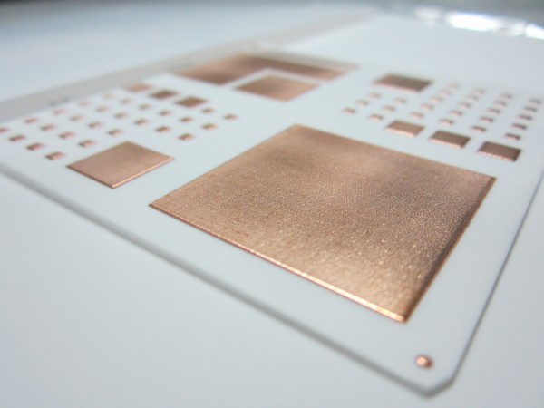
Ordinary PCBs are typically made by bonding copper foil to a substrate, with most substrates composed of materials like fiberglass (FR-4) or phenolic resin (FR-3), and adhesives usually being phenolic or epoxy. In contrast, ceramic substrates are primarily made of metal oxide ceramics such as aluminum oxide (Al₂O₃), beryllium oxide (BeO), and aluminum nitride (AlN), resulting in significant differences in performance between the two.

Differences Between Ceramic PCB and Ordinary PCB
Compared to traditional printed circuit boards (PCBs), ceramic circuit boards offer numerous advantages. Due to their high thermal conductivity and minimal coefficient of thermal expansion (CTE), ceramic circuit boards feature more functions, simpler structures, and superior performance compared to conventional PCBs.

Advantages and Disadvantages of Ceramic PCB
Advantages:
Disadvantages:
Types of Ceramic PCBs
High-Temperature (HTCC)
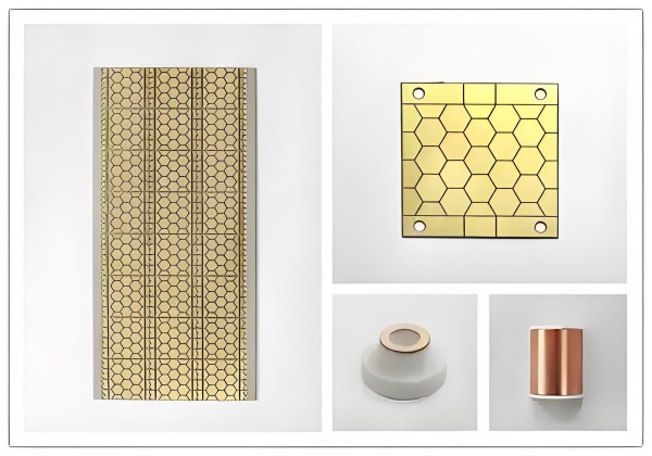
Perhaps the most popular type of ceramic PCB is the high-temperature PCB. Ceramic circuit boards designed for high temperatures are often called high-temperature co-fired ceramic (HTCC) circuits. These circuits are constructed by mixing binders, lubricants, solvents, plasticizers, and aluminum oxide to form green ceramic.
Using the produced green ceramic material, the material is then coated, and circuit traces are made on tungsten or molybdenum metal. After lamination, the circuit is baked at temperatures between 1,600 and 1,700 degrees Celsius for up to 48 hours. All HTCC baking is performed in a gas environment, such as hydrogen.
Low-Temperature (LTCC)
Unlike HTCC, low-temperature co-fired ceramic (LTCC) PCBs are made by mixing crystalline glass with bonding materials on a metal plate and gold paste. The circuit is then cut and laminated before being placed in a gas oven at approximately 900 degrees Celsius.
LTCC PCBs benefit from less warping and improved shrinkage resistance. In other words, they offer excellent mechanical strength and thermal conductivity compared to HTCC and other types of ceramic PCBs. When using heat-dissipating products like LED lights, LTCC's heat-dissipation advantages provide a significant benefit.
Thick-Film Ceramic
Thick-film ceramic circuits involve applying gold and dielectric pastes on a ceramic base material. Once applied, the paste is baked at 1,000 degrees Celsius or lower. Due to the high cost of gold conductor paste, this type of PCB is popular among major printed circuit board manufacturers.
The main advantage of thick-film ceramic materials over traditional PCBs is their ability to prevent copper oxidation. Therefore, if a ceramic PCB manufacturer is concerned about oxidation, choosing thick-film ceramic circuits can be beneficial.
A common question is, "How many layers does a ceramic PCB have?" The answer depends on the type of ceramic PCB used. The minimum number of layers in a ceramic PCB is two, but more layers may be added depending on the product's performance requirements. A width calculator helps manufacturers understand their PCB design specifications.
Applications of Ceramic PCBs
Memory Modules
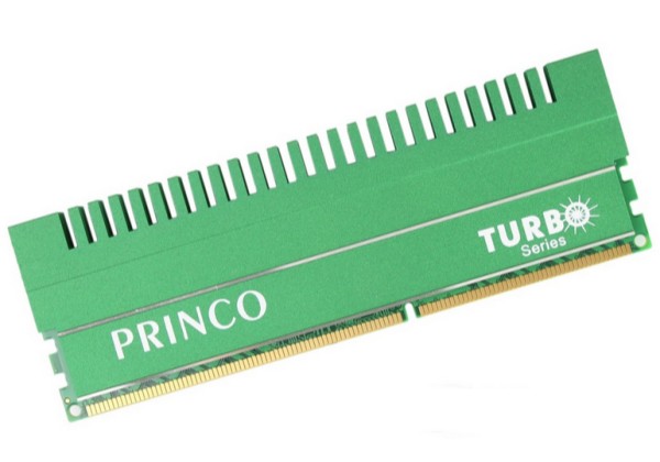
One of the key application areas for ceramic PCBs is memory modules. These PCBs house memory integrated circuits and are commonly used in producing DDR SDRAM and other memory-related computer components. All RAM used in personal computers requires ceramic substrate PCBs with integrated memory modules.

Transmit and Receive Modules
Ceramic PCBs enable the production of radar technology. Westinghouse was the first company to use multi-layer ceramic PCBs to create transmit and receive modules due to their high thermal conductivity and compatible CTE. Unlike conventional PCBs, ceramic circuits are the only option for creating transmit modules.
Multi-Layer Interconnection Boards
One of the main selling points of ceramic PCBs is their higher capacity than conventional circuit boards. In other words, ceramic PCBs can accommodate more components using the same surface area compared to traditional PCBs. Therefore, ceramic PCBs with multi-layer interconnection boards have more potential applications.
Analog/Digital PCBs
Various computing companies use low-temperature ceramic circuit (LTCC) boards to create advanced analog and digital boards with excellent circuit tracing capabilities. Personal computer companies have leveraged LTCC to create many lightweight circuits, reducing overall product weight and minimizing crosstalk.
Solar Panels
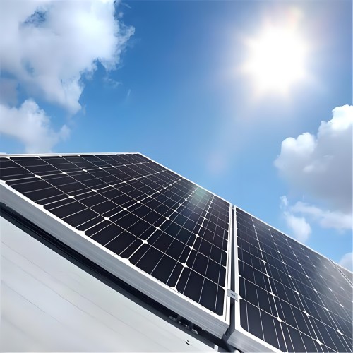
Both HTCC and LTCC are used in manufacturing solar panels and other photovoltaic (PV) electrical panels. Photovoltaic panels utilize multi-layer ceramic board technology to ensure service life and adequate thermal conductivity.

Power Transmitters
Wireless power transmission and charging modules are becoming increasingly common in consumer electronics. These devices are built using ceramic PCB technology due to their unique thermal properties and heat-dissipating ceramic substrates.
Ceramic circuit boards generate electromagnetic fields through which energy is transmitted between receivers and transmitters. Induction coils help transfer electricity from the original electromagnetic field and convert it into current for receiver circuits, which are typically made of ceramic-based PCB materials.
Semiconductor Coolers
An increasing number of electronic devices are being miniaturized, driven by semiconductor chips that become smaller every year. Semiconductor chips use microfabrication technology to achieve higher high-speed integration while maintaining optimal tracing capabilities.
Traditional PCBs cannot meet the circuit requirements of modern semiconductor chips. However, the emergence of ceramic-based semiconductor circuits has enabled superior integration and performance between microcircuit components. Therefore, ceramic PCB substrates are often regarded as the future of semiconductor technology.
High-Power LEDs
Ceramic substrates provide the optimal base for high-power LED lights. Unlike traditional PCBs, ceramic circuits use thick-film technology to maximize thermal efficiency. As a result, the heat generated by LED lights (approximately 70% of an LED's energy) does not affect the circuit's efficiency.
In other words, only ceramic circuits can provide the thermal efficiency level required for LED lighting. When LEDs are built on ceramic circuits, thermal interface materials (also known as heat sinks) are unnecessary. Therefore, manufacturers can use fewer materials to produce and maintain LED lights when using ceramic circuits.
Types of Ceramic PCB Materials
Aluminum Oxide (Al₂O₃)
Also known as metal substrate PCBs, aluminum oxide PCBs use dielectric thermal-conductive and electrically insulating materials between aluminum metal and copper layers. It is the preferred PCB for anything involving heat dissipation and overall temperature maintenance and control.
The aluminum structure typically consists of three layers: a copper circuit layer (1 to 10 ounces thick), an insulating layer made of thermal-conductive and electrically insulating material, and a base layer made of copper or aluminum metal substrate.
There are several types of aluminum PCBs, including flexible, hybrid, multi-layer, and through-hole types.
Aluminum Nitride (AlN)
AlN, also known as aluminum nitride, is a new material developed to be commercially viable, with reproducible and controllable properties over the past two decades.
AlN is an effective choice due to its good dielectric properties, low thermal expansion coefficient, high thermal conductivity, and non-reactivity with common semiconductor process chemicals.
Aluminum nitride PCBs are typically used in heat sinks, microwave device packaging, molten metal processing components, substrates for electronic packaging, and semiconductor processing chamber fixtures and insulators, to name a few applications.


