HDI PCB: Manufacturing, Layout & Benefits Guide
 21 Apr 2025 17:58:09 GMT
PCBASAIL
What is HDI PCB?
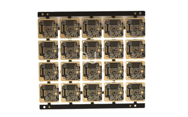
HDI board (High Density Interconnector) is a type of printed circuit board (PCB) manufactured using micro blind/buried via technology, featuring a high-density circuit layout. Designed as a compact product for small-capacity users, it adopts a modular parallel design: each module has a capacity of 1000VA (1U height), uses natural cooling, and can be directly installed in a 19” rack, with a maximum of 6 modules in parallel. HDI boards have inner and outer circuit layers, and through processes such as drilling and via metallization, connections are achieved between layers.

Why Use HDI PCBs?
HDI PCBs offer numerous technical advantages over surface mount technology (SMT) and through-hole boards:
Design Flexibility:
Compared to SMT or through-hole boards, HDI boards provide designers with greater flexibility. Designers can leverage high component density to enable faster signal processing.
Smaller Footprint: Thanks to advanced technical features, HDI boards can easily accommodate more connections with fewer layers on the same board.
Reliability:
HDI boards have smaller vias and lower aspect ratios (AR), making them more reliable than traditional through-hole vias.
Suitability for Dense and Complex Packaging: HDI is the preferred choice for dense and complex packaging involving high pin counts and fine pitches. HDI boards are typically manufactured using a build-up process—the more build-up layers, the higher the technical grade. Standard HDI boards use 1 build-up layer, while high-order HDI employs 2 or more layers, along with advanced PCB technologies like stacked vias, electroplated filled vias, and direct laser drilling. When PCB density exceeds eight layers, manufacturing with HDI is cheaper than traditional complex lamination processes.
Growing Demand for Miniaturized PCBs:
HDI boards meet the rising demand for smaller PCBs. Non-HDI boards require more space and weight, limiting their use in many scenarios. Multiple PCBs can also be integrated into a single HDI board. As electronic products evolve toward higher density and precision, HDI technology enables more compact terminal designs while meeting stricter standards for electrical performance and efficiency. Popular electronic products such as mobile phones, digital cameras, laptops, and automotive electronics often use HDI boards.
Signal Integrity:
The advanced technical features of HDI PCBs improve signal integrity and electrical performance, making them preferable to SMT or through-hole boards. HDI boards facilitate advanced packaging technologies and offer higher electrical performance and signal accuracy than traditional PCBs. Additionally, they provide better mitigation of radio frequency interference (RFI), electromagnetic interference (EMI), electrostatic discharge (ESD), and thermal management.
How to Set Up HDI PCB Layout
HDI PCB Layout
For HDI PCBs, little distinguishes them from standard PCBs except for component and routing density. Some designers define HDI boards as those with vias of 1000μm or smaller, traces of 600μm or smaller, or pin pitches of 0.5mm or smaller. Manufacturers may specify that HDI PCBs use blind vias of ~8 mils or smaller, with laser drilling for the smallest vias.
In some ways, all these definitions are valid, as there is no universal threshold for what constitutes an HDI layout. Everyone agrees that once a design includes microvias, it is an HDI board. From a design perspective, you must first set specific design rules before starting the layout. Before establishing these rules, gather your manufacturer’s capabilities. Once done, define design rules and layout features:

Trace Width and Via Size: Trace width affects impedance and determines whether you’re entering HDI territory. As trace widths shrink, vias must shrink too, often requiring microvia fabrication.
Layer Transitions: Vias must be carefully designed based on aspect ratios, which depend on desired layer thicknesses. Define layer transitions early to facilitate rapid placement during routing.
Clearance: Traces must be spaced apart and separated from other non-network objects (pads, components, planes, etc.). The goal is to comply with HDI DFM rules and prevent excessive crosstalk.
Other Routing Constraints: Factors like trace length tuning, maximum trace length, and allowable impedance deviations are important but apply beyond HDI boards. The two most critical points here are via size and trace width. Clearance can be determined through simulations or standard rules of thumb, but exercise caution with the latter to avoid excessive crosstalk or insufficient routing density.
Stackup and Vias
HDI stackups can range from a few layers to dozens, adapting to required routing density. Boards with high-pin-count fine-pitch BGAs may have hundreds of connections per quadrant, necessitating careful via planning when creating a layer stackup for HDI layout.
If your PCB design software’s layer stack manager does not explicitly define microvia layer transitions, don’t worry—you can still set layer transitions and then apply via size constraints in design rules. This ability to designate microvias via design rules is particularly useful for creating templates. To set routing rules for microvias, define rules that apply only to microvias, allowing specific constraints on pad size and hole diameter.
Before setting design rules, consult your manufacturer about their capabilities. Then, set trace widths in design rules to ensure impedance control meets requirements. Even when impedance control isn’t required, limiting trace widths on HDI boards can help maintain high routing density.

Quality Issues and Solutions in HDI Manufacturing
Poor Solderability
Poor solderability, especially in batch issues, is a critical problem. Possible causes include:
Contamination or oxidation on the board surface
Abnormal black nickel plating or nickel thickness
Solder mask scum (shadowing) on pads
Excessive storage time leading to moisture absorption
Solder mask covering pads or thick repairs
Contamination and moisture issues are relatively easy to resolve, but other problems require stricter process control. For example, black nickel plating issues may stem from outsourced gold plating, inadequate analysis of plating solution concentrations, or lack of regular gold stripping tests and phosphorus content checks. To prevent batch issues, ensure the PCB manufacturer follows strict process controls and quality assurance plans, such as regular solderability testing and clear standards for repair limits (e.g., no repairs in dense pad areas like BGAs or QFPs).
Delamination
Delamination is a persistent issue in PCBs, often caused by:
Improper packaging/storage leading to moisture absorption
Exceeding shelf life and moisture ingress
Supplier material or process defects
Poor material selection or copper distribution in design
Moisture-related delamination can often be mitigated by baking boards at 120°C for 4 hours before use if humidity indicators are exceed standards. Supplier-related issues like poor brown/black oxidation, wet prepreg (PP) or inner layers, insufficient PP resin, or lamination defects may require scrapping. To reduce risks, verify the manufacturer’s process controls and reliability testing (e.g., thermal stress testing requiring ≥5 cycles without delamination for high-quality factories, versus ≥2 cycles for ordinary ones). Designers should also select materials with Tg ≥145°C and avoid large copper areas or dense buried via regions.
Scratches and Copper Exposure
This defect reflects a manufacturer’s management and execution. While not always critical, it poses quality risks. Improvement hinges on proactive measures: pushing the PCB factory to implement special projects, strengthen process discipline, and improve operator training and inspection standards.
Board Warpage/Twist
Causes include:
Poor material selection by the supplier
Process anomalies during production
Improper rework control
Inadequate transportation/storage
Weak breakaway tab design
Unbalanced copper area across layers
Design reviews should address breakaway tab strength and copper area balance. Require manufacturers to simulate reflow soldering (IR) conditions to test warpage. For thin boards, specify protective packaging with wooden boards and use fixtures during SMT to prevent sagging.
Impedance Variations
Consistent impedance is critical for RF performance in mobile phone boards. Common issues include batch-to-batch impedance variations. Since impedance test strips are typically on panel edges and not shipped with boards, request suppliers to provide test strips and reports for each batch, along with data comparing trace widths on panel edges and inner layers.


