High-Frequency PCBs: From Theory to Production
 18 Apr 2025 16:39:31 GMT
PCBASAIL
Definition of High-Frequency PCB
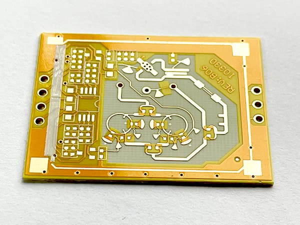
A high-frequency PCB refers to a type of high-frequency component produced using standard FR4 rigid PCB manufacturing processes on specific high-frequency copper-clad substrates. When selecting high-frequency materials, key factors to consider include: dielectric constant and its tolerance (Dk), dissipation factor (Df), coefficient of thermal expansion (CTE), peel strength, and water absorption rate.

Currently, the most widely used high-frequency materials in the world are mainly from two American brands—ROGERS and TACONIC. Their base materials are primarily polytetrafluoroethylene (PTFE), also known as Teflon. These PCBs are often referred to as PTFE PCBs, F4, or by various transliterations like "Teflon", "Teflon board", etc. In terms of frequency, high-frequency generally refers to frequencies above 1GHz.
Is High-Frequency PCB Just Expensive?
It’s true that high-frequency PCBs are costly—around USD 2468 per square meter—but their performance is far beyond that of standard PCBs.
Key Features of High-Frequency PCBs
Low Dielectric Constant
A lower and more stable dielectric constant means better signal stability. In high-frequency applications, this ensures excellent signal transmission. It also has very low dielectric loss, low water absorption, and is heat- and corrosion-resistant. Conversely, a higher dielectric constant results in slower signal transmission.
Thermal Expansion Coefficient
The thermal expansion coefficient of the high-frequency board must match that of the copper foil as closely as possible. Mismatches can lead to copper foil separation due to thermal cycling, affecting signal transmission reliability.
Low Water Absorption
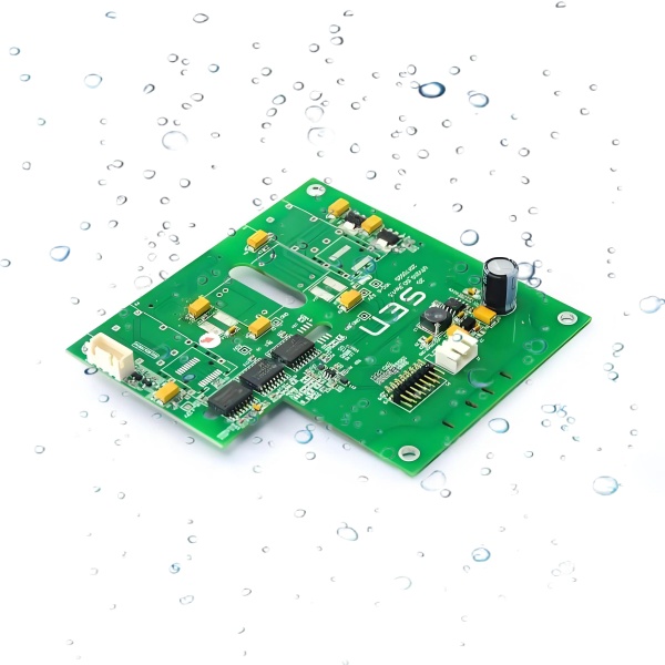
High-frequency PCBs have lower water absorption compared to other multilayer boards. Moisture can affect the dielectric constant and dissipation factor. Therefore, properties like heat resistance, chemical resistance, impact strength, and peel strength must also be excellent.
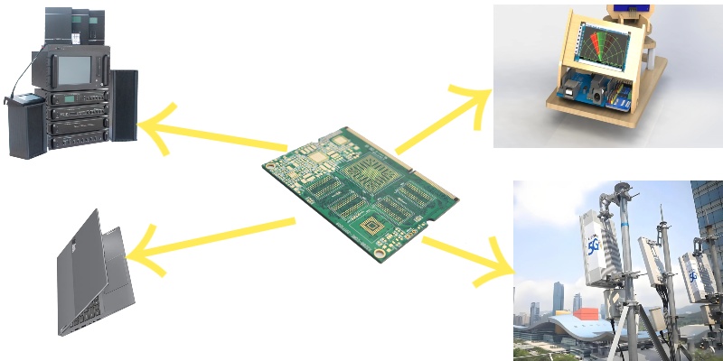
High-frequency PCBs have high demands for physical properties, precision, and technical parameters. They are commonly used in automotive collision avoidance systems, satellite systems, radio systems, and more.

Application Fields of High-Frequency PCBs
High-frequency PCBs can be categorized into two main application areas:
High-frequency signal transmission electronic products: These involve electromagnetic waves and transmit signals using sine waves, such as microwave, RF, radar, broadcasting, and communication systems.

High-speed logic signal transmission electronic products: These rely on digital square wave transmission, initially used in computers and now widely applied to home appliances and communication electronics.
Common High-Frequency PCB Materials
Currently, high-frequency substrates fall into three major resin types: epoxy resin, PPO resin, and fluorinated (PTFE) resin. Epoxy is the cheapest, while fluorinated resin is the most expensive. From the standpoint of dielectric properties and frequency performance, fluorinated resin is the best, and epoxy the worst.
When operating frequency exceeds 10GHz, only fluorinated resin substrates are suitable. While PTFE-based materials have excellent electrical properties, they suffer from high cost, poor rigidity, and a high CTE (coefficient of thermal expansion).
To improve these, PTFE substrates are often filled with inorganic materials like silica (SiO₂) or reinforced with fiberglass fabric to enhance rigidity and reduce thermal expansion.
Special Processing Considerations for PTFE PCBs
Due to the chemical inertness of PTFE molecules, bonding with copper foil is difficult. Surface treatment is essential and can include chemical etching, plasma etching, or adding a bonding film layer between the copper and PTFE to improve adhesion. However, this may slightly impact dielectric performance.
The development of fluorinated high-frequency substrates requires joint collaboration between raw material suppliers, research institutions, equipment providers, PCB manufacturers, and end-product producers to keep pace with the rapidly evolving needs of high-frequency circuitry.
High-Frequency PCB Manufacturing Process
Due to the unique requirements of high-frequency PCBs—fast signal propagation, low loss, high stability, resistance to temperature extremes, solvents, etc.—customers often pre-evaluate these characteristics during product design.
Material Selection: Material selection should be based on electrical properties such as DK and DF per the customer’s specifications.
A. Copper Foil Selection:
For high-frequency antenna boards:
RTF (Reverse-Treated Foil): Rz ≤ 5.1 μm
RA (Rolled Annealed Foil): Rz ≤ 3 μm
B. Common High-Frequency Materials:
Refer to material specification tables. Thickness tolerance should meet IPC-4103 Class B standards.
1.2 Process Flows
A. NPTH (Non-Plated Through Hole) PTFE Board Process:
Cutting → Drilling → Image Transfer → Etching → Inspection → Solder Mask → Silkscreen → Profiling → Testing → Final Inspection → Immersion Tin → Final QC → Packaging → Shipping
·Positive Image Process:
Cutting → Drilling → Hole Preparation (including PTFE through-hole treatment) → Electroless Copper → Plating → Image Transfer → Inspection → Pattern Plating → Alkaline Etching → AOI → Solder Mask → Silkscreen → Profiling → Testing → Final Inspection → Immersion Tin → Final QC → Packaging → Shipping
Negative Image Process:
Cutting → Drilling → Hole Preparation → Electroless Copper → Plating → Image Transfer → Inspection → Acid Etching → AOI → Solder Mask → Silkscreen → Profiling → Testing → Final Inspection → Immersion Tin → Final QC → Packaging → Shipping
C. Multilayer Pure PTFE or Hybrid Stack-Up Process:
Cutting → Inner Layer Image Transfer → Etching → Browning (bake inner core at 110°C for 2 hours after browning) → Lamination → Drilling → Hole Treatment → Electroless Copper → Outer Layer Image Transfer → Pattern Plating → Alkaline Etching → Solder Mask → Silkscreen → Profiling → Testing → Final QC → Immersion Tin → Final QC → Packaging → Shipping
Notes:
a. Thermoset ceramic hydrocarbon materials (non-PTFE) follow similar processing steps as standard FR-4 materials. PTFE-based boards, however, require adjustments in drilling, plating, solder mask, and routing stages.
b. All NPTH holes must be drilled before etching.
c. Surface finish costs vary from high to low: ENIG, immersion silver, soft gold, lead-free HASL, immersion tin, HASL with lead, OSP. (Note: tin spraying is not recommended.)
d. If quality requirements allow, PTFE boards (especially those without solder mask or silkscreen) can be profiled before etching, then surface treated, to avoid edge burrs. Alternatively, consider two-stage profiling (before and after etching).


