How PCBASAIL Assembly PCB Board Step By Step
 08 Apr 2025 14:41:43 GMT
PCBASAIL
How PCBASAIL Assembly PCB Board Step By Step
With the continuous development of electronic technology, electronic products have been widely used in various fields of life. However, PCB production and assembly is an important part of product production. We found that many customers, whether they are engineers entering the industry or experienced professionals, do not fully understand the process of PCB production and assembly. In order to let customers better understand how we transform their PCB design data into the final high-quality PCBA board, I will share entire production process from raw material preparation to PCB patch assembly to show our professional production technology and how we ensure the reliability and performance of each PCB board we produce.
What Files We Need To Assembly PCB Board?
In the PCB production and assembly process, in order to ensure that we can correctly produce the PCBA board we need, we must prepare all the files required for production. These files include PCB files, drilling files, BOM (Bill of Materials), assembly drawings and other requirements, etc.
PCB Files
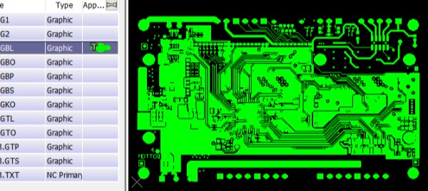
The PCB tool we commonly use include Altium Designer: .PcbDoc, KiCad: .kicad_pcb, Eagle: .brd, and Gerber files format (RS-274X) file is the main file for PCB production, which contains the graphic information of each layer of the PCB.
1)Top Layer and Bottom Layer)
2)Inner layers
3)Solder Mask
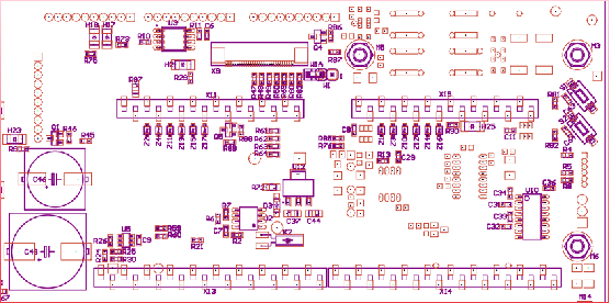
4)Silkscreen
5)Drill File
6)Board Outline

BOM List
BOM (Bill of Materials): BOM is an indispensable file for component procurement and assembly, mainly in Excel or CSV file format. BOM needs to contain detailed information of all components required for PCB
Part Number
Description
Package Type
Quantity
Reference Designator

3,Pick and Place Files
The coordinate file is preferably in the text file CSV or TXT format, which is used to help SMT accurately mount BOM electronic components. It contains the component designator, X coordinate, Y coordinate, component installation direction, component package, and whether the component is located on the top or bottom of the PCB.

4,Assembly drawings
Assembly Drawing: Although it is not an essential document, a detailed assembly drawing can help us check whether the components are correctly mounted and avoid assembly errors. It is mainly in the form of PDF or DXF files and contains the following information
Reference Designator
Polarity Markings
Install Orientation

5,Firmware programming and function test
We hope to help customers test and burn. Customers only need to provide the tools and methods required for firmware and burning test. Our engineers will burn and test all PCB boards before shipment to ensure that the PCB boards can operate normally. Potential problems can be found through testing, reducing rework and repair costs, and avoiding delays or failures of customer projects due to PCB problems.
What Machines we use for PCB assembly
In the whole PCB assembly process, we need to use a lot of equipment, so what equipment is our production workshop equipped with?
Solder Paste Printer
Solder Paste Detection Instrument
Pick and Place Machine
Reflow Oven
First Article Tester
AOI Equipment (Automated Optical Inspection)
X-Ray Inspection Equipment (X-Ray Inspection Machine)
Wave Soldering
Dry Ice Cleaning Machine
What steps for PCB assembly?
Step 1-Material preparation:
We need to prepare the already produced PCB bare board, PCB steel mesh, BOM components (SMD components, DIP components or other components required for assembly) and related procedures
Step 2-Solder Paste Application:
Our automatic printer will print solder paste on the PCB bare board through the steel mesh
This is the first step of PCB assembly. Solder must be added before adding components. It is required to add solder only to the area of the circuit board where solder is to be applied. Apply the solder to the board with the help of a solder sieve, place its steel mesh in the correct position on the board, and apply the scraper tin on it. This allows the solder to be squeezed out of the hole and applied to the circuit board
Step 3-Solder Paste Inspection (SPI):
Check the quality of solder paste printing, whether there are boards with poor printing,
Step 4-Components Pick and Place:
Our technicians debug the program, and the SMT machine automatically grabs and mounts the components. This is done after tinning. Surface mount technology (SMT) requires precise placement of components, which is difficult to achieve through manual placement. Therefore, the components are placed on the circuit board with the help of a pick and place machine. The location where the components need to be placed and the component information required by the pick and place machine are provided in the PCB design information.
Step 5-Reflow Soldering:
Adjust parameters such as the furnace temperature and perform the furnace. After placing the components, the circuit board is placed on the reflow oven conveyor. The solder applied during the tinning process will melt during the reflow soldering process, which will permanently connect the components to the circuit board.
Step 6-Assembly Inspection: Visual inspection and AOI inspection, screening and repair of defective products
Step 7-Final Testing and Validation Burning Test
Step 8-Final Assembly and Packaging Packaging and Shipping
PCBASAIL is equipped with 5 SMT production lines and 1 wave soldering post-welding line to ensure efficient and high-quality PCB assembly. Each SMT production line includes a solder paste printer, SPI equipment, a high-speed placement machine, a reflow oven and AOI equipment, which supports the placement and welding of high-precision and high-density components. The wave soldering post-welding line is equipped with a plug-in machine, a wave soldering machine and a detection equipment, which is specially designed for through-hole component welding. The overall production capacity reaches 1,200-2,900 PCBs per hour to meet diverse production needs.


