Drilling Thick Copper PCBs: Overcoming Challenges & Improving Quality
 07 Apr 2025 15:51:31 GMT
PCBASAIL
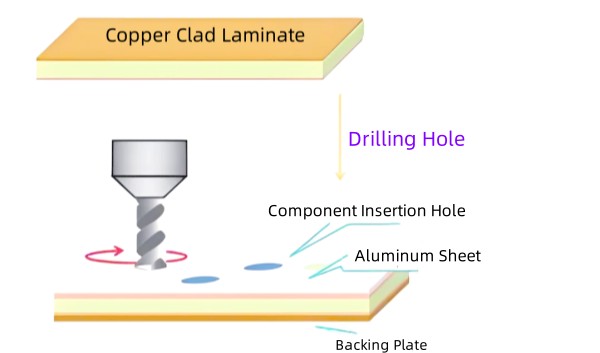
In the field of PCB manufacturing, thick copper plates have become the core base material for power modules, high-power electronic devices, and industrial control systems due to their excellent electrical conductivity and heat dissipation performance. As the thickness of the copper layer jumps from the conventional 1-3 ounces to 6 ounces or even higher, its processing technology faces unprecedented challenges. Drilling, as a key process in PCB production, presents unique physical phenomena and process contradictions in the processing of thick copper plates: on the one hand, the high thermal conductivity significantly reduces the cutting temperature; on the other hand, the plastic deformation characteristics of copper materials lead to secondary problems such as copper wire entanglement and copper adhesion. Behind this contradiction is a complex game of interactions among materials science, machining, and thermodynamics.

I. The Thermodynamic Paradox of Drilling Thick Copper Plates
The thermal conductivity of copper is as high as 401 W/(m·K), approximately 1.8 times that of aluminum and 5 times that of iron. During the drilling process, the heat generated in the cutting area is quickly conducted and dispersed through the copper matrix. Theoretically, it can effectively suppress the temperature rise of the tool and the workpiece. This characteristic brings twofold advantages: the tool wear rate is reduced by about 30%, and the positional accuracy deviation caused by thermal deformation is reduced by more than 50%, which is especially suitable for the processing of high-precision multi-layer boards. However, this seemingly ideal heat dissipation characteristic hides a mystery - when the drill bit cuts in, the instantaneous plastic flow of the copper material will form a high-pressure area in front of the cutting edge. Although the overall temperature is low, the frictional heat at the microscopic contact points can still reach the recrystallization temperature of copper (about 200°C) instantaneously.
This phenomenon leads to the dynamic softening of the surface layer of the copper material, forming a viscous metal flow. When the rotational speed of the drill bit exceeds 80,000 RPM, the contact time between the chip and the rake face of the tool is shortened to the microsecond level. However, the ductility of the copper chips makes it difficult for them to break effectively. Instead, under the action of centrifugal force, long spiral chips are formed. These copper wires are wound between the drill shank and the chip evacuation groove, not only hindering the penetration of the coolant but also generating secondary frictional heat. Experimental data shows that when the thickness of the copper layer exceeds 4 ounces, the local temperature rise caused by the copper wire entanglement phenomenon can reach 40% of the basic cutting temperature, forming a paradoxical effect of "low-temperature cutting - local high temperature".
II. The Generation Mechanism of Material Plastic Behavior and Processing Defects
The elongation rate of pure copper is as high as 45%. This excellent plasticity is manifested as a three-stage deformation characteristic during the drilling process: lattice slip in the initial shearing stage, dislocation proliferation in the plastic flow stage, and necking phenomenon before fracture. When drilling thick copper plates, due to the increase in the axial cutting depth, the material removal process is closer to the orthogonal cutting model, and the shear plane angle is reduced to 15°-25°, resulting in a 30%-50% increase in chip thickness. During the discharge process of these thick and continuous chips, their free surfaces intermittently contact the hole wall, forming a dynamic process of periodic adhesion - tearing.
The essence of the copper adhesion phenomenon is interfacial metallurgical bonding. When the cutting temperature reaches the recrystallization temperature of copper, atomic diffusion occurs between the fresh copper surface and the tool surface under high pressure. Even if the overall temperature is low, the instantaneous temperature of the microscopic protrusions can exceed 500°C, which is sufficient to trigger a small amount of fusion welding. When using a tungsten carbide drill bit, the precipitation of the cobalt bonding phase will accelerate this adhesion. EDX analysis shows that the cobalt content in the adhered substance can reach 8.3wt%, forming a Co-Cu intermetallic compound. The shear strength of this metallurgical bonding layer is as high as 350MPa, which is 3 times the strength of pure copper itself, resulting in a negative deviation of the effective rake angle of the tool and a surge in the cutting force by more than 25%.
III. The Collaborative Optimization of Process Parameters and Tool Design
Breaking through the dilemma of drilling thick copper plates requires the construction of a multi-dimensional process control system. First of all, in terms of cutting parameters, the strategy of "high rotational speed - low feed rate" has a contradiction: increasing the rotational speed to 90,000 RPM can reduce the feed per tooth to 0.01mm, which is beneficial to thinning the chip thickness, but the increase in centrifugal force exacerbates the risk of copper wire entanglement. The latest research shows that by using the variable frequency oscillating feed technology and superimposing an axial vibration of 10-50Hz, the chip breakage length can be shortened by 70%. In combination with a pulsed cooling system, high-pressure coolant (pressure 7MPa) is injected during the vibration return stroke, which can effectively remove the accumulated chips in the chip evacuation groove.

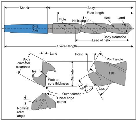
The innovative design of the tool geometric parameters is even more crucial. Reducing the rake angle of the drill tip from the conventional 30° to 15° will increase the cutting force, but it can enhance the edge strength and suppress plastic flow. Adjusting the helix angle from 40° to 35°, while maintaining the chip evacuation ability, reduces the spiral curvature radius of the chip and promotes chip breakage. The "double waveform edge" technology developed by a German tool manufacturer processes periodic ripples with a wavelength of 0.8mm and an amplitude of 0.05mm on the cutting edge, causing the chips to generate forced bending strain, and the fracture probability is increased to 92%. In terms of coating technology, multi-layer composite coatings show unique advantages. A 1μm-thick CrN is used as the bottom layer to improve the bonding strength, a 0.5μm-thick MoS₂ solid lubricating layer is used as the middle layer, and a 2μm-thick diamond-like carbon film (DLC) is deposited on the surface layer. This structure reduces the friction coefficient from 0.6 to 0.15, and the adhesive force is reduced by 80%. A Taiwanese PCB manufacturer uses this coated drill bit to process 6-ounce thick copper plates, and the tool life is increased from 1,200 holes to 4,500 holes, and the Ra value of the hole wall roughness is controlled within 1.6μm.
IV. New Opportunities Brought by Material Modification
Material engineers are seeking breakthroughs from the copper foil itself. Adding 0.3%-0.5% of tellurium element to form a Cu-Te alloy can, while maintaining the electrical conductivity (≥85%IACS), increase the tensile strength to 350MPa and control the elongation rate at about 15%. This treatment of moderately reducing plasticity shortens the chip breakage length by 40%. Another innovative direction is to develop anisotropic copper foils. Through the rolling process, the grains are oriented in the drilling direction, and the crystallographic texture effect is used to reduce the transverse plasticity. Tests show that for this copper foil during the processing of a 0.3mm hole diameter, the incidence rate of copper wire entanglement is reduced by 65%.
The nano-structured surface treatment technology provides a new idea for breaking through the problem of copper adhesion. Micro-pit arrays (diameter 20μm, depth 5μm, spacing 50μm) are processed on the surface of the copper foil by laser texturing. These micro-structures can serve as lubricant reservoirs and continuously release nano-molybdenum disulfide particles. During the drilling process, these solid lubricants form a transfer film at the tool - workpiece interface, reducing the interfacial shear strength to 1/3 of that of the pure copper system. Experimental data from a Japanese research institute shows that this method reduces the axial force during drilling by 28% and the adhesive wear amount by 90%.
V. The Closed-loop Control of the Intelligent Manufacturing System
Under the framework of Industry 4.0, the drilling process of thick copper plates is evolving towards digital closed-loop control. By integrating multi-physical field sensors, multi-dimensional data such as spindle current (sensitivity ±0.1A), acoustic emission signals (frequency range 50-500kHz), and infrared thermal images (spatial resolution 0.1mm) are monitored in real-time. A cutting state recognition model is established using deep learning algorithms. When the characteristic frequency of copper wire entanglement (usually in the frequency band of 120-180kHz) is detected, the system automatically adjusts the spindle torque output and triggers a high-pressure air knife (pressure 0.8MPa) for on-line chip removal.

The adaptive control system is more forward-looking. The intelligent drilling machine developed by an American equipment manufacturer can dynamically adjust the processing strategy according to the thickness of the copper layer: for a copper layer of 4-6 ounces, a constant force feed mode is adopted to maintain the cutting force within the range of 120-150N; when the copper layer exceeds 6 ounces, it is switched to the step-by-step drilling mode, first pre-drilling with 0.8 times the hole diameter, and then completing the final drilling with a stepped feed. This strategy reduces the tool load fluctuation by 40% and improves the hole position accuracy to ±25μm.
VI. The Diverse Evolution of Future Technology Routes
Laser drilling technology is breaking through the limitations of traditional machining. The combination of picosecond laser (pulse width 10ps) and annular spot technology can achieve micro-hole processing with a taper of less than 2° on a 100μm-thick copper layer, and the heat-affected zone is controlled within 5μm. Although the current cost is 3-5 times that of mechanical drilling, it has begun to replace traditional processes in the field of high-density interconnection. The combined processing solution shows greater potential: first, use a laser to process a guide hole (diameter 0.05mm), and then use a micro-drill for precise expansion. This combined process increases the processing efficiency by 70% and reduces the tool wear by 90%.

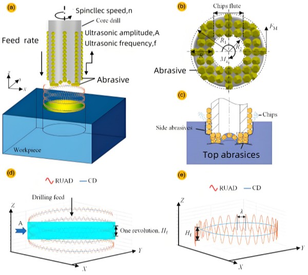
The ultrasonic-assisted drilling technology has entered the practical stage. A 40kHz ultrasonic vibration device is integrated on the spindle, making the drill bit generate a high-frequency vibration with an axial amplitude of 5μm. This vibration makes the cutting process show the characteristic of "intermittent cutting", effectively releasing the cutting stress periodically. When processing an 8-ounce thick copper plate, the axial force is reduced by 35%, and the chip thickness is thinned to 1/3 of that of the conventional process. A more revolutionary breakthrough comes from cold cutting technology. Using liquid nitrogen (-196°C) jet to locally freeze the cutting area makes the copper material undergo a brittle transition and achieve a brittle fracture mode. Preliminary tests show that this method can completely eliminate the phenomenon of copper wire entanglement, but it is necessary to solve the problem of dimensional shrinkage compensation caused by low temperature.
Today, as PCB technology continues to develop towards high power and high density, the solution to the problem of processing thick copper plates has gone beyond simple process improvement and has evolved into an innovative arena of interdisciplinary integration. From the research on the interfacial behavior at the molecular dynamics level to the intelligent control of the macroscopic manufacturing system, every technological breakthrough is redefining the limits of electronic manufacturing. In the future, with the maturity of new material technologies such as superconducting copper alloys and quantum dot lubricants, as well as the development of atomic-level manufacturing processes, the drilling of thick copper plates will leap from the "problem-solving" stage to the "performance design" stage, opening up a new era for the miniaturization and high efficiency of electronic devices. This game between copper and the drill bit will ultimately drive the entire electronic manufacturing industry to evolve to a higher dimension.


