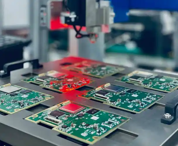
Introduction to pcb assembly process
 19 Feb 2025 15:58:25 GMT
PCBASAIL
PCB (Printed Circuit Board) assembly process is the process of mounting electronic components onto a PCB in accordance with design requirements to form a circuit board with specific functions. The following is a detailed description of the PCB assembly process:
First, pre-preparation
Components and materials procurement
Bill of Materials (BOM): According to the design requirements of the PCB, list all the required electronic components and materials.
Procurement: According to the BOM, purchase qualified components and materials. If there are unobtainable components, they can be replaced by similar components with the buyer's consent.

PCB Manufacturing
Manufacturing process: Including inner layer line production, lamination, drilling, hole metallization, outer dry film, outer layer line, silk screen, surface process and other steps, finally forming a bare board without any components installed.
Quality control: During the manufacturing process, the PCB is subjected to strict quality inspection to ensure that the board's dimensions, lines, holes, etc. meet the design requirements.
Assembly Documentation Preparation
Assembly documents: including BOM, Gerber documents, Pnp documents, PCBA test documents, etc., to ensure that there is a complete reference and guidance in the assembly process.
Drawings: provide PCB manufacturing drawings and assembly drawings, clear bare board specifications and assembly instructions.
Second, assembly process
Solder paste application
Principle: similar to the stencil printing T-shirt, through the machine with the help of the stencil will be applied to the surface area of the PCB where the components will be placed in the future.
Operation: Place the template on the PCB and roll it with a roller, the solder paste enters the pads and holes.
Component placement (pick and place)
Method: Manual placement or machine operation. In order to improve the speed and accuracy, the machine is usually used to pick up and place the components automatically.
Requirements: Ensure that the components are accurately placed on the pads to avoid shifting and skewing.
Reflow Soldering
Purpose: Melt solder paste to form a reliable electrical and mechanical connection between component pins and PCB pads.
Process: The PCB is fed into the reflow oven where the solder paste melts and solidifies at high temperature.
Plug-in component insertion
Object: components that require through-hole insertion, such as electrolytic capacitors, high-power components.
Method: Manual or automated equipment inserts components into the through-hole of the PCB.
Wave soldering
Purpose: Melt the solder to form the electrical connection of the through-hole inserted components.
Process: so that the PCB through the melted solder wave, solder and component pins and PCB pad connection.
Third, detection and testing
Quality Inspection
Visual inspection: check the quality of welding from the appearance, such as whether the solder joints are smooth, there is no continuous welding, bridge welding, etc..
Hand touch inspection: touch the components by hand to check whether they are loose.
Machine Inspection: Use X-ray inspection and automatic optical inspection (AOI) and other technologies to check for welding defects, misalignment, leakage of stickers and other problems.
Functional Testing
In-Circuit Testing (ICT): Through test equipment, the electrical properties of circuit boards, such as resistance, capacitance, voltage, etc., are examined.
Function Test (FT): Verify whether the function of the circuit board meets the design requirements, such as signal transmission, data processing, etc.
Fourth, post-processing
Cleaning
Purpose: to remove residual flux and other pollutants in the welding process to ensure that the PCB surface is clean.
Mode: chemical cleaning or ultrasonic cleaning and other methods.
Assembly and Testing
Installation of shell: According to the design requirements, install the shell of the circuit board and protection devices.
Final Test: Verify the overall function and performance of the product to ensure compliance with customer requirements.
Packing and Shipping
Cleaning & Packaging: Clean, package and label qualified products.
Anti-static and moisture protection: Take necessary measures to prevent product damage during transportation and storage.
Shipping: Send the products to customers.
Fifth, assembly skills and precautions
Ensure that the silkscreen is clear
Role: Silk-screen marking is used to indicate the placement of components, component polarity, test points and other information, and must be clear and legible.
Marking component polarity
Requirements: On components such as electrolytic capacitors, LEDs, diodes and ICs, clearly identify the cathode and anode, as well as marking the 1-pin to prevent errors during assembly.
Segregation of leaded and lead-free components
Reason: Lead-free components cannot be mixed with those not designated for lead-free assembly to ensure solder quality and compliance.
Pay attention to component spacing
Requirement: Avoid spacing components too close to each other during assembly and creating assembly problems. Different types of components have different spacing requirements between them.
Even placement of large components
Purpose: To allow even heat distribution during reflow soldering to ensure soldering quality.
Perform DFM inspection
Purpose: Identify design errors at an early stage to prevent problems such as rework and repair at a later stage. Mainly can identify component spacing, polarity, packaging and other assembly problems.
Through the above steps and techniques, you can ensure the smooth running of the PCB assembly process, improve product quality and productivity.


