The Evolution of SMT
In the 1970s and 1980s of the 20th century, the level of automation in electronic product manufacturing gradually increased. Using traditional components and wires was not easy. Resistors and capacitors needed their leads to be pre-formed so that they could fit into through-holes. Sometimes, even tools were needed to set their leads at proper intervals to make them pass through holes better.
For printed circuit board (PCB) technology, there's no need for component leads to go through the board. Instead, it's enough to solder components directly onto the board surface. So, Surface Mount Technology (SMT) came into being. The use of SMT components developed rapidly because their advantages were realized and put into practice.
How SMT Works
Simply put, SMT works like this: print solder paste on fixed points of a PCB, then use machines to place components like resistors and capacitors on the board surface. After that, the board goes through a furnace for high-temperature baking to cure the solder paste. This makes the components firmly soldered to the board, forming a complete circuit board assembly. This technology is used in the production of electronic devices we use daily, such as mobile phones, computers, and tablets.
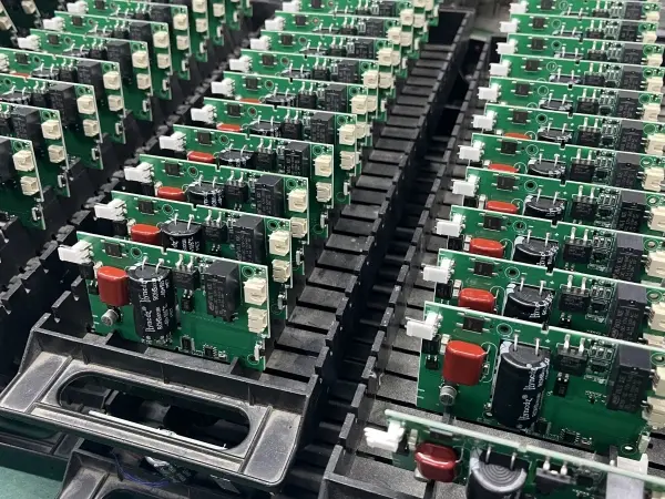
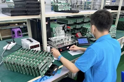
SMT Personnel at PCBASAIL
Each step in SMT is a separate position:
SMT Equipment
Processing Equipment:
Solder paste printers, pick-and-place machines, and reflow ovens
Testing Equipment:
SPI (Solder Paste Inspection) and AOI (Automatic Optical Inspection)
Auxiliary Equipment:
SPI (Solder Paste Inspection) and AOI (Automatic Optical Inspection)
Typical SMT Production Line Layout
loader → solder paste printer → solder paste inspection equipment (SPI) → pick-and-place machine → pre-furnace AOI → reflow oven → post-furnace AOI → rework station → unloader
Single-rail or double-rail conveyors are used between these machines to transfer PCBs.
Key SMT Equipment and Their Functions
Solder paste printer
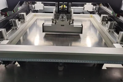
Solder paste is placed on a pre-designed stencil. A mechanical arm controls a scraper to push the solder paste from one end of the stencil to the other. The solder paste leaks through the stencil holes, falling onto the corresponding positions on the PCB under the stencil.
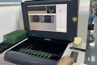
Solder paste inspection equipment (SPI)
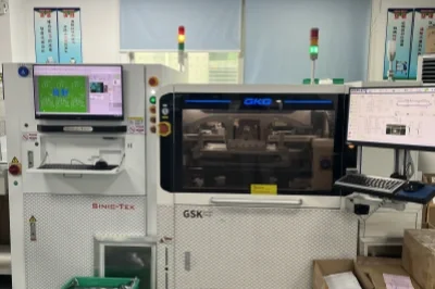
Uses optical principles to check the quality of printed solder paste. It prevents issues like missing prints, insufficient solder, excess solder, solder bridging, misalignment, poor shape, and board surface contamination.
Pick-and-place machine
Uses nozzles to pick up component materials, then controls the mechanical arm to place the materials on the correct positions on the PCB surface.
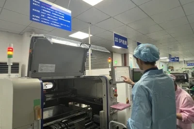
AOI
Uses optical detection to check component placement. It looks for problems like misalignment, missing components, wrong polarity, skewing, and wrong parts. After reflow soldering, it checks for issues like insufficient solder, excess solder, misalignment, and poor shape.
Reflow oven
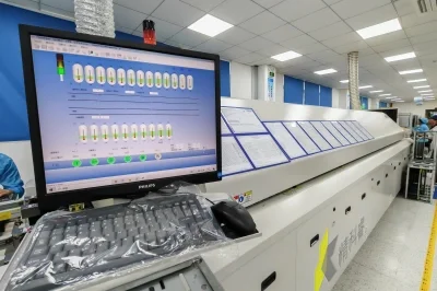
Has different temperature zones. It uses hot air or infrared radiation to create temperature gradients in the oven. When the PCB goes through the oven, the solder paste cures as the temperature rises and falls.
Loaders, unloaders, and conveyors
These are used to transfer PCBs between different stages of the production line, ensuring smooth and continuous workflow throughout the SMT process.
Rework station
Has basic heating functions. It is a workbench for manual inspection and rework of soldered PCBs, equipped with tools to correct defects and ensure product quality.
Applications of SMT
SMT is widely used. For example, the smartphones everyone holds today are circuit boards produced using this process. Later, through final assembly, circuit boards, cameras, thermal conductive glue, adhesive glue, screens, and other materials are assembled into a mobile phone.
Smartphones
Computers
Tablets
Companies like Foxconn, Huawei, OPPO, VIVO, Xiaomi, and BYD all have their own SMT lines. These large electronics manufacturers also work with many contract manufacturers. For example, Foxconn is Apple's most well-known contract manufacturer.
Advantages of SMT
- High assembly density, small product size, and light weight. The size and weight of surface mount components are only about 1/10 of traditional through-hole components. Generally, after using SMT, the volume of electronic products is reduced by 40%~60%, and the weight is reduced by 60%~80%.
- High reliability and strong vibration resistance. The rate of solder joint defects is low.
- Good high-frequency performance. It reduces electromagnetic and radio frequency interference.
- Easy to automate, improving production efficiency.
- Reduces costs by 30%~50%. It saves materials, energy, equipment, labor, and time.
Disadvantages of SMT
- Equipment accuracy can't reach 100%. Errors still occur, leading to scrapping of soldered PCBs.
- Manual intervention, inspection, and rework are needed for the equipment.
- Complex and precision parts have the risk of aging and damage, which may stop the production line.
- Data platforms of equipment from different manufacturers are incompatible with each other.
Common SMT Process Defects
1. Tombstoning (Manhattan Phenomenon)
Phenomenon
One end of a chip component (such as 0402, 0603 resistors and capacitors) lifts up, while the other end is soldered to the pad, looking like a "tombstone."
Causes
The pads at both ends of the component are asymmetric in size (difference in heat capacity); uneven solder paste amount; too fast heating during reflow.
Solutions
Optimize PCB design; ensure uniform solder paste printing; adjust the reflow profile to reduce heating rate.
2. Bridging (Soldering Stage)
Phenomenon
Solder between adjacent solder joints connects, causing a short circuit.
Causes
Excess solder paste; too small pin spacing of components; too high fluidity of solder paste; too small distance between PCB pads.
Solutions
Reduce solder paste printing amount; use low-fluidity solder paste; lower reflow peak temperature; optimize PCB pad design.
3. Cold Solder Joints
Phenomenon
Solder joints look dull and rough, with weak bonding (easy to fall off) and poor electrical contact.
Causes
Oxidation of pads/component pins; insufficient activity of flux in solder paste; too low reflow temperature or too short time.
Solutions
Clean PCB pads and component pins; use high-activity flux; adjust the reflow profile to increase peak temperature.
4. Solder Balls
Phenomenon
Small solder balls scatter around solder joints, which may cause potential short circuits.
Causes
Solder paste is squeezed out of pads during printing; flux in solder paste volatilizes too fast; solder paste not fully stirred.
Solutions
Control printing pressure; optimize the reflow preheating zone; fully stir solder paste before use.
5. Solder Joint Voids (Air Pores)
Phenomenon
Bubbles appear inside or on the surface of solder joints (common in BGA, QFP solder joints).
Causes
Volatiles from flux in solder paste not discharged in time; oil on pads/pins; insufficient solder paste.
Solutions
Extend time in the reflow preheating zone; strengthen cleaning of PCBs and components; increase solder paste amount appropriately.
6. Wave Soldering Spurs (Needle-like Protrusions)
Phenomenon
Sharp solder spurs appear at the end of solder joints (common in through-hole components).
Causes
Too high wave height (excess solder); insufficient flux spraying; too slow speed when PCB leaves the wave.
Solutions
Lower the wave height; increase flux spraying amount; increase PCB transmission speed.
Requirements for SMT Workshop Production Environment
Many people who use SMT equipment for the first time are not familiar with the requirements for the working environment of SMT production equipment. Here are some environmental requirements from PCBASAIL for reference. First, it's important to note that SMT production equipment is high-precision electromechanical equipment. The equipment and process materials have certain requirements for environmental cleanliness, humidity, and temperature.
Factory Building Requirements
- • Load capacity: >8KN/m²
- • Vibration: controlled within 70dB (max 80dB)
- • Noise: controlled within 70dBA
Power Supply
- • Single-phase AC220 (220±10%, 50/60Hz)
- • Three-phase AC380 (380±10%, 50/60Hz)
- • Power supply capacity: >twice the power consumption
Air Source
- • Pressure: >7kg/cm²
- • Clean, dry purified air (oil, dust, and water removed)
- • Stainless steel or pressure-resistant plastic pipes
Ventilation
Reflow soldering and wave soldering equipment need exhaust fans. For full hot air ovens, minimum exhaust flow rate: 500 cubic feet per minute (14.15m³/min).
Lighting
Ideal illumination: 800~1200LUX (minimum 300LUX). Local lighting for inspection, rework, and measurement areas.
Working Environment
- • Cleanliness: Class 500,000
- • Temperature: 23±3℃ (17~28℃)
- • Relative humidity: 45%~70%RH
- • Temperature and humidity monitoring required
PCBASAIL's SMT Capabilities
PCBASAIL has four fully automatic SMT placement lines with a daily production capacity of 8 million points; automatic assembly lines, wave soldering, and DIP insertion lines with a daily production capacity of 400,000 pieces; and 4 assembly lines that can adapt to the assembly of various large, medium, and small equipment products.
Component Expertise
We have expertise in placing and reworking components such as QFP, TQFP, PLCC, QFN, LGA, BGA, and more.
Anti-static Measures
We have complete anti-static production measures to ensure component protection during manufacturing.
Quality Control
Effective control of key process links including IQC, IPQC, and OQA inspections.
Our Advantages
Equipped with a team of electronic engineers who monitor and adjust at any time, effectively improving product quality and production efficiency.
Our Guarantee
We have passed the ISO9001 quality management system and support the placement of precision electronic components. Your trust and support will drive us forward, and we will offer you our best prices in return.
Contact Us
For any PCBA requests, please contact our marketing department by email:
We'll never let you down.
Our Services Include:
- SMD mounting: YAMAYA SMT Machine
- DIP assembly: Manual soldering for small batches, wave soldering for mass production
- Cleaning: All PCBA are cleaned by a dry icing machine to avoid damage to components.
BGA Assembly Quote
Get your customized pricing