What is BGA?
As market demands for chip integration increase, the number of I/O pins has risen sharply, and power consumption has also grown. This has made integrated circuit packaging more stringent. To meet these development needs, BGA Assembly began to be used in production.
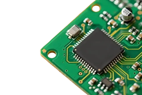
BGA, also known as Ball Grid Array packaging technology, is a high-density surface-mount packaging technology. Spherical bumps are formed in an array on the back of a printed substrate to replace pins. An LSI chip is mounted on the front of the printed substrate, which is then sealed using molding resin or potting.
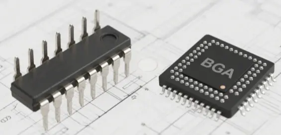
It is also called a Bump Array Carrier (PAC). It can have more than 200 pins, making it a packaging option for multi-pin LSI chips. The pins are spherical and arranged in a grid-like pattern, hence the name BGA. The solder balls act as the connection interface between the packaged IC and the PCB. Their connection is achieved using SMT (Surface Mount Technology).
Key Insight
BGA technology revolutionized packaging by replacing traditional pins with an array of solder balls on the bottom of the package, enabling higher pin counts without sacrificing reliability or manufacturability.
History of BGA Assembly
Early BGA Assembly
Early BGA Assembly mainly used plastic materials. This packaging method had low costs and was suitable for consumer electronics. However, plastic BGA had low thermal conductivity, which limited its use in high-performance computing and communication devices.
Ceramic BGA Assembly
To solve the thermal conductivity issue, ceramic BGA Assembly technology emerged. Ceramic materials have higher thermal conductivity, allowing them to better conduct heat generated by the chip to the circuit board. This improves the chip’s reliability and performance.
High-Density BGA Assembly
As electronic devices demand higher performance and integration, high-density BGA Assembly technology came into being. This technology achieves higher I/O density by increasing the number of solder joints and reducing their spacing. This allows chips to integrate more functions.
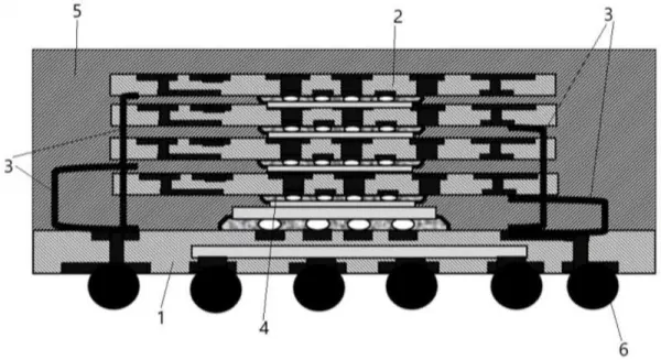
3D Stacked BGA Assembly
To further save space and improve performance, 3D stacked BGA Assembly technology began to appear. This technology stacks multiple chips vertically, achieving higher integration and faster data transmission speeds.
Characteristics of BGA Assembly Technology
Currently, most motherboard control chipsets use this packaging technology, often with ceramic materials. Memory packaged using BGA technology can double or triple its capacity without changing its volume. Compared to TSOP, BGA has a smaller size, better heat dissipation, and better electrical performance.
Characteristics of Two BGA Assembly Technologies
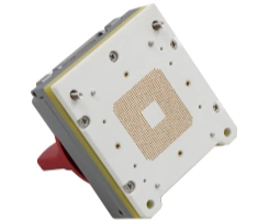
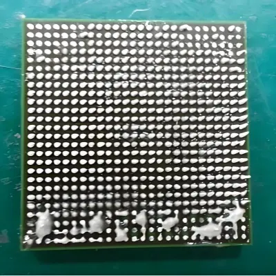
BGA Packaged Memory
The I/O terminals of BGA packaging are distributed in an array of circular or columnar solder joints under the package. A key advantage of BGA technology is that although the number of I/O pins increases, the pin pitch does not decrease—in fact, it increases. This improves assembly yield.
While power consumption rises, BGA can use controlled collapse chip connection (C4) soldering, which improves its thermal and electrical performance. Its thickness and weight are both reduced compared to previous packaging technologies. Parasitic parameters are smaller, signal transmission delay is shorter, and the operating frequency is significantly higher. Assembly can use coplanar soldering, resulting in high reliability.
TinyBGA Packaged Memory
Memory products using TinyBGA packaging have a volume only 1/3 that of TSOP packaging for the same capacity. TSOP packaged memory has pins drawn out from around the chip, while TinyBGA has pins drawn out toward the center of the chip.
This effectively shortens signal transmission distance—the length of signal transmission lines is only 1/4 that of traditional TSOP technology. As a result, signal attenuation is reduced. This not only greatly improves the chip’s anti-interference and anti-noise performance but also enhances its electrical performance.
Substrate Requirements
The substrate or interposer is a very important part of BGA Assembly. Besides being used for interconnect wiring, it can also be used for impedance control and integration of inductors/resistors/capacitors. Therefore, substrate materials need to have a high glass transition temperature (Tg, approximately 175~230℃), high dimensional stability, low moisture absorption, good electrical performance, and high reliability. There must also be high adhesion between the metal film, insulating layer, and substrate medium.
Advantages and Applications of BGA Assembly
BGA Assembly technology has been widely used in the electronics industry due to its unique advantages. Below are some key advantages and their application areas.
Key Advantages
High I/O Density
BGA Assembly technology can provide high I/O density. This means more pins can be integrated into the same chip area, enabling higher data transfer rates and more complex functions. This advantage has made BGA Assembly widely used in high-performance computing, high-speed communication, and complex system integration.
Good Thermal Management
Compared to traditional Pin Grid Array (PGA) packaging, BGA Assembly has better thermal management capabilities. Spherical solder joints provide a larger contact area, helping to conduct heat. This is crucial for high-performance processors, Graphics Processing Units (GPUs), and other devices that require good heat dissipation.
Mechanical Stability
The spherical solder joints of BGA Assembly are more mechanically stable than traditional pin packaging. They can better absorb thermal expansion and mechanical stress, reducing the risk of solder joint breakage and thus improving product reliability.
Space Saving
Since BGA Assembly’s solder joints are distributed on the bottom of the chip, circuit board design becomes more flexible, saving valuable space. This is particularly important for mobile devices, wearable devices, and other applications with strict space requirements.
Application Areas
Consumer Electronics
BGA Assembly technology is widely used in smartphones, tablets, laptops, and other devices to achieve high performance and compact design.
Automotive Electronics
As cars become more electronic, BGA Assembly plays an important role in in-vehicle infotainment systems, Advanced Driver Assistance Systems (ADAS), and battery management systems for electric vehicles.
Industrial Control
In industrial automation and control systems, BGA Assembly’s high reliability and performance make it an ideal choice.
Communication Equipment
In high-speed communication devices such as 5G base stations, routers, and switches, BGA Assembly technology is used to achieve high-speed data processing and signal transmission.
Three Main BGA Assembly Processes and Flows
1. Wire Bonded PBGA Assembly Process Flow
PBGA Substrate Preparation
Very thin copper foil (12~18μm thick) is laminated on both sides of a BT resin/glass core board. Then, drilling and via metallization are performed. Conventional PCB processes are used to create patterns on both sides of the substrate, such as conductive strips, electrodes, and arrays of solder ball pads. A solder mask is then applied and patterned to expose the electrodes and pads. To improve production efficiency, a single substrate usually contains multiple PBGA substrates.
Assembly Process Flow
2. FC-CBGA Assembly Process Flow
Ceramic Substrate
The substrate for FC-CBGA is a multi-layer ceramic substrate, and its production is quite difficult. This is because the substrate has high wiring density, narrow spacing, many vias, and strict coplanarity requirements. The main process is: first, high-temperature co-firing of multi-layer ceramic sheets to form a multi-layer ceramic metallized substrate. Then, multi-layer metal wiring is created on the substrate, followed by electroplating, etc. In CBGA assembly, the mismatch in Coefficient of Thermal Expansion (CTE) between the substrate, chip, and PCB is the main cause of CBGA product failure. To improve this, besides using a CCGA structure, another type of ceramic substrate—HITCE ceramic substrate—can be used.
Assembly Process Flow
3. Wire Bonded TBGA Assembly Process Flow
TBGA Carrier Tape
TBGA carrier tape is usually made of polyimide material. During production, copper is clad on both sides of the carrier tape, followed by nickel and gold plating. Then, via punching, via metallization, and patterning are performed. In this wire-bonded TBGA, the package heat sink serves as both the package reinforcement and the base of the package cavity. Therefore, before packaging, the carrier tape is bonded to the heat sink using a pressure-sensitive adhesive.
Assembly Process Flow
The main reason for the popularity of BGA Assembly is its obvious advantages. Its unique strengths in packaging density, electrical performance, and cost have allowed it to replace traditional packaging methods. Over time, BGA Assembly will see more improvements, and its cost performance will further increase. With its flexibility and excellent performance, BGA Assembly has a broad future.
BGA Assembly Soldering: Common Defects and Anomaly Analysis
Solder Ball Fracture
This is a common issue in BGA soldering, mainly caused by improper control of soldering temperature or equipment vibration. If the soldering temperature is too high, the solder ball may expand excessively, leading to fracture. If equipment vibration is too strong, it may increase mechanical stress on the solder ball, causing fracture.
Cold Solder Joint
Another common problem, cold solder joints are characterized by a poor metal connection at the solder point. Main causes include poor solder wettability, soldering temperature below the solder paste melting point, or solder contamination during soldering.
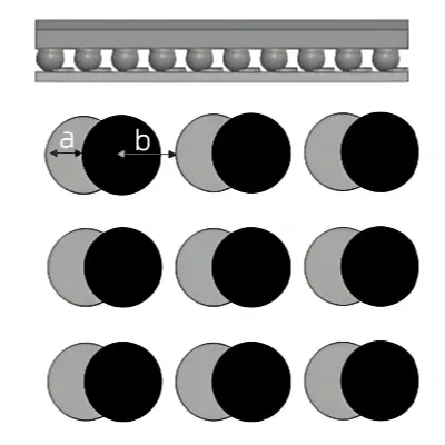
Solder Ball Misalignment
During soldering, solder balls may shift due to thermal expansion, uneven surface tension, or other factors, reducing connection quality. Especially in high-density BGA Assembly, even small shifts can cause serious performance issues.
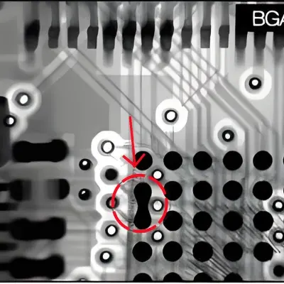
Bridging
If there is too much solder or excessive solder flow, bridging may occur. This is an unwanted electrical connection between two or more solder points. Bridging not only affects normal circuit operation but may also cause short circuits, damaging the device.
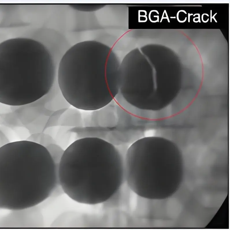
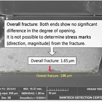
Post-Soldering Cracks
These are cracks that appear during or after soldering, caused by soldering stress, thermal cycle stress, or mechanical vibration. Such cracks may lead to circuit breaks, affecting device reliability.
Appearance Defects
During BGA soldering, appearance defects such as uneven solder surfaces or darkened solder color may occur. These are generally caused by improper setting of soldering process parameters, poor control of environmental temperature and humidity, or poor solder quality. While these defects may not directly affect circuit board functionality, they can reduce its lifespan and reliability.
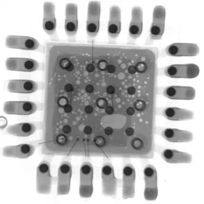
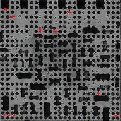
Internal Defects
Using X-rays or other non-destructive testing technologies, internal defects in BGA soldering may be found, such as holes or cracks inside solder balls. These internal defects may result from gas generation and trapping during soldering, or uneven shrinkage during solder cooling. They can affect circuit electrical performance and reduce fatigue and vibration resistance.
Poor Post-Soldering Electrical Performance
Some defects cannot be detected by visual inspection or X-rays and only appear in electrical performance tests. For example, poor soldering quality may lead to increased resistance, current fluctuations, or signal delays. These issues can severely affect circuit board performance and may even render it inoperable.
There are many common defects and anomalies in BGA Assembly soldering, and each can affect circuit board performance and reliability. Therefore, strict control of the BGA soldering process is crucial. This requires strict process parameter settings, high-quality soldering materials, precision soldering equipment, and rigorous quality inspection and control. By gaining a deep understanding of common defects and anomalies in BGA Assembly soldering, we can better control the soldering process and improve circuit board quality and reliability.
BGA Applications
BGA Assembly is widely used across various fields due to its advantages. In consumer electronics, it is essential for smartphones and laptops, enabling compact designs with powerful performance. In automotive electronics, it supports the complex functions of ADAS and battery management systems, ensuring stable operation under harsh vehicle conditions.
In industrial control, its high reliability makes it suitable for automation equipment that requires long-term stable operation. In communication devices, especially 5G technology, BGA Assembly’s high-speed data transmission capabilities help meet the demands of fast communication.
With the continuous development of electronics, BGA Assembly will find even more applications, driving innovation in electronic products.
Future Trends
- Higher density with smaller solder ball pitches
- 3D integration for increased functionality
- Improved thermal management solutions
- Enhanced reliability for extreme environments
Key Growth Areas
- 5G and next-generation communication systems
- Artificial intelligence and machine learning hardware
- Automotive advanced driver assistance systems
- High-performance computing and data centers
BGA Assembly Quote
Get your customized pricing