Why PCB Design Needs Mechanical Collaboration
 20 May 2025 14:29:26 GMT
PCBASAIL
A perfect electronic product cannot be achieved solely with excellent PCB (Printed Circuit Board) design. Just as beautiful flowers need fine brocade and a good horse needs a suitable saddle, the electronic part of the PCB carrying your ingenious design inspiration also requires precise mechanical parts and casing design to match, as well as careful processing and polishing in PCB manufacturing and assembly. The organic collaboration among these teams is essential to successfully deliver a perfect electronic product.
The cooperation between electronic and mechanical design teams runs through the entire PCB design process via 3D component libraries, including the matching design of mechanical casings related to the circuit board in the later design stage. The manufacturing and assembly stages also require component list (BOM) information from design data and must comply with both electronic and mechanical design requirements. The organic collaboration of these teams can significantly improve product yield, shorten development time, and effectively avoid many potential issues.
Electronics and Mechanics in PCB Design
In PCB design, component mounting inevitably requires considering the mechanical dimensions, size, height, and volume of components to achieve precise PCB layout design. The overall board shape and corresponding mounting holes must also match the mechanical casing. After PCB manufacturing and assembly, the three-dimensional dimensions of the physical circuit board must ensure compatibility with the mechanical casing from all angles.
Ordinarily, if the electronic and mechanical design teams cannot unify and interact data in real time, you will surely be familiar with and troubled by the following scenarios. For example, you may manually measure component dimensions to design PCB footprints.
When multiple PCBs need to be nested and assembled, you must accurately calculate the size
and position of the grooves to be cut on each PCB to avoid assembly failures.

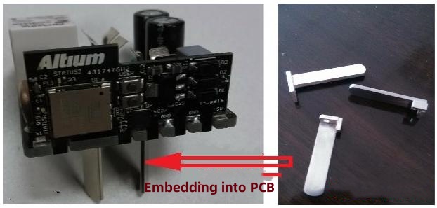
After the circuit boards are prototyped, assembled, and tested, manual visual inspection is required to check for spatial conflicts between components, between boards, and between connectors. As shown in the figure below, do the pins of PCBs align horizontally and vertically? Is there any spatial conflict between large energy-storage capacitors/relays and other objects? Are the dimensions of the three metal pins of this WIFI-controlled smart power socket reasonable? Does their mounting match the circuit board? These electronic-mechanical matching issues alone require countless rounds of revisions between PCB design and mechanical design!
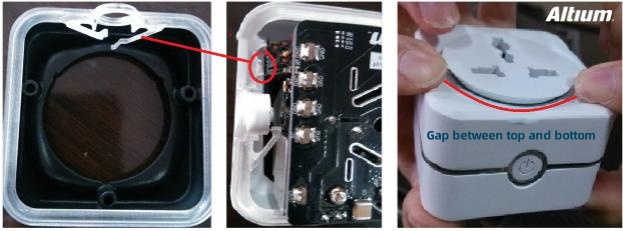
Next is the matching between the assembled PCB (electronic core) and the product casing. The
smart power socket has a transparent plastic light-transmitting strip in the middle of the
casing (left figure below). Two photosensors are positioned on the light-transmitting strip
opposite the power button, corresponding to two LEDs on the vertically assembled PCB. The
intended effect is that the LEDs emit RGB-colored light strips in different states and can
be used as night lights. However, due to spatial conflicts, one of the plastic photosensors
was crushed by the LED!

Finally, when the entire casing is installed, a gap is found between the upper cover and the main body, failing to fit perfectly!
These problems can be avoided in Altium Designer. When creating component library footprints,
automatically generating STEP models ensures the spatial coordination of components on the
PCB. ECAD-MCAD collaboration ensures the matching between the electronic core and the
mechanical casing.

PCB Design and Manufacturing
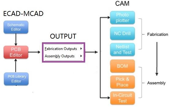
After completing PCB design, files need to be exported for downstream PCB manufacturing and assembly. Outputs are divided into two parts: Fabrication Outputs (manufacturing files) and Assembly Outputs (assembly files).
PCB manufacturers use Gerber files or ODB++ files exported from Altium Designer to obtain PCB drawing data. They also require NC Drill data, Netlist, and test data. These files and data must be packaged and sent to the manufacturer along with processing requirements.
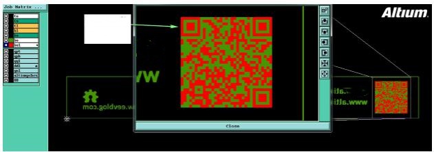
The manufacturer will list questions for communication and confirmation with engineers based
on the received data and processing requirements. For example, confirming the color of the
silk-screened QR code on the PCB (see figure below for the effect of changing red to black
solder mask).

During confirmation, Altium’s Draftsman documentation tool is used for effective communication and intent transmission. After reaching a consensus, PCB production, processing, and testing can proceed.
The figure below shows some of the equipment required for PCB manufacturing. There are many processes and equipment involved in PCB processing; only a few automatic production line devices are listed here for a general overview. For detailed production processes and technical details, consult professionals at each processing factory.
PCB Design and Assembly
Similar to the design-to-manufacturing stage, the design-to-assembly stage requires Altium Designer to package and export Assembly Outputs for assemblers, including BOM (bill of materials), Pick-and-Place files for chip mounters, and In-Circuit Test (ICT) files.
In fact, within Altium Designer, the PCB layout and routing stage already matches component models and mechanical parts (such as product casings) to ensure correct component models/sizes and compatibility between the assembled PCB (electronic core) and the mechanical casing. As shown in the figure below, this power strip contains 8 socket modules, each with electronic components (resistors, capacitors, relays, transformers, etc.) and PCBs perfectly matched to their mechanical casings.
During PCB assembly, as long as the bare PCBs, electronic components, and other parts meet design requirements (with clear BOM lists and guaranteed quality), the process of component placement, soldering (per Pick-and-Place files), and other assembly steps becomes standardized and precise. After all components are assembled, ICT and functional tests are performed.
The figure below shows some assembly production line equipment. PCB assembly includes SMT component placement and soldering, connector placement and soldering, product testing, surface treatment and protective coating application, and packaging (sometimes combined with mechanical casing assembly). Altium Designer must provide accurate BOM lists, Pick-and-Place files, stencil files, etc., for automated placement. Additionally, collaboration with assembly manufacturers is required to provide test files, configure test fixtures, and inspect product yield.
If data sharing and collaboration among PCB electronic design, mechanical design, manufacturing, and assembly teams are insufficient, post-assembly discovery of mismatches between electronic components and mechanical casings will require redesigning either the PCB or the casing. Each revision involves modifying design data, reprocessing, and re-matching, which is time-consuming and labor-intensive for all teams. Therefore, to avoid such iterative rework, a perfect electronic product must integrate all teams during the design stage, share data, and ensure organic collaboration to prevent data errors and potential issues.