Why Do Capacitors Come in Strange Shapes?
In the PCB world, you will see many kinds of capacitors. You know some of them already. For example, through-hole ceramic capacitors, single-chip ceramic capacitors, MLCC (multi-layer ceramic capacitors), and parts in sizes like 1206, 0805, 0603. Many people have seen those. Now look at the pictures below. You may not have seen these shapes before.
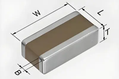
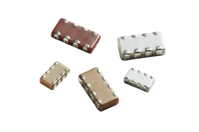

All of those parts are ceramic capacitors. They look strange because their package shapes changed over time. The change in package is not just for looks. It is tied to how power is supplied and cleaned in modern digital circuits. Today I will not teach you how to use every new capacitor type. Most people will never need most of them. Instead, I will explain why these new shapes appeared. Knowing the background will help you understand how they are used in the power distribution network (PDN). It is like learning about tanks to better know how attackers and defenders fight on the battlefield.
Trends in Digital Circuits
Digital chips keep getting denser. Process nodes shrink. Speed goes up. Power goes up. Core voltages go down. These trends will likely continue. One result is that PDN integrity becomes a bigger problem.
When chips switch, they draw very fast pulses of current. The PDN must give stable voltage to each chip pin. If the PDN has high impedance at some frequency, the switching current makes voltage ripple and noise. That noise can cause wrong logic or make the chip reset. So designers must control PDN impedance. The goal is to keep impedance below a target across the current spectrum of the system.
What is the Power Distribution Network (PDN)?
The PDN is all the conductors and parts that deliver power from a regulator to active devices on the PCB. It includes:
- The regulator or voltage module.
- Power and ground planes on the PCB.
- Traces from the plane to pads and vias.
- Vias and their inductance.
- Chip package leads, balls, and bond wires.
- Chip internal wiring and its distributed inductance and capacitance.
- Large bulk capacitors and the distributed capacitance of the PCB.
- Any filter parts and decoupling capacitors.
Every piece has resistance, inductance, and capacitance. Many of these values are small. Yet they matter a lot at high frequency. The PDN is not an ideal zero-ohm DC source. Its AC impedance changes with frequency and with where you measure it.
Why Impedance Matters
Key Principle
When a chip switches, current flows through PDN impedance. The product of current and impedance creates voltage noise. Lower impedance = less noise.
In a perfect PDN, voltage to each chip is always constant. The AC impedance between power and ground would be zero. In real life, impedance is never zero. When a chip switches, it draws a fast current pulse. The current flows through the PDN impedance. The product of current and impedance creates a voltage change. This change is switching noise. The noise size depends on PDN impedance. So the rule is simple:
Designers must keep PDN impedance low where the chip draws current.
If you fail, you get more ripple and jitter. The chip may reset or misbehave.
How to Lower PDN Impedance
You can lower PDN impedance in many ways. Here are the common ones:
- Use wider power traces. Wider traces have less resistance and less inductance.
- Add filter capacitors and decoupling capacitors at many locations.
- Use multiple layers with a power plane and a ground plane close to each other. A pair of planes form a good distributed capacitor.
- Use multiple vias to reduce via inductance and resistance.
- Use capacitors with low equivalent series inductance (ESL).
- Place decoupling capacitors as close to chip power pins as possible. Make the loop from capacitor to pin short and wide.
The last two points are critical. In high-speed design, one key rule is:
Pick capacitors with low equivalent inductance. Then make the decoupling loop inductance as small as possible.
Many layout techniques aim to lower loop inductance. For example, put capacitors near the power pin, shorten the traces, make traces wider, and use nearby vias. We will not list all layout tricks here. Instead, I will explain the physics behind them. That will make the reason for the new capacitor shapes clear.
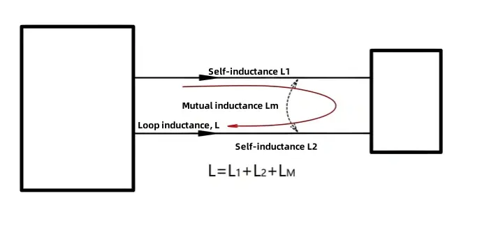
Loop Inductance & Mutual Inductance
A capacitor is not just capacitance. It always has some series resistance and series inductance. At high frequency, inductance kills the capacitor's effective capacitance. In some cases, the capacitor can act like an inductor at high frequency.
The two traces that connect the capacitor to the power and ground form a current loop. The
loop has self-inductance (each trace) and mutual inductance (between the traces). The total
loop inductance equals the sum of the two self-inductances plus or minus twice the mutual
inductance, depending on current directions. If the currents in the two conductors flow in
opposite directions, the total inductance is roughly the sum of self-inductances minus the
mutual inductance. When the traces are close, mutual inductance is large and cancels self
inductance, so the total loop inductance is low. That helps the capacitor work at high
frequency.
So to reduce loop inductance:
- Shorten traces (lower self-inductance).
- Put the two traces close together (increase mutual inductance and cancel self-inductance).
This is the basic reason to keep decoupling capacitors close to power pins and to route power and return traces tightly together.
How Capacitor Makers Reduced Inductance
Capacitor vendors took the same approach. They changed package forms to lower the capacitor's own inductance. Here are the main methods.
1) Make the capacitor smaller
A smaller package usually has lower inductance. That is why MLCCs moved from bigger sizes like 1206 down to 0805, 0603, 0402, and smaller. Small caps can be placed closer to chip pins. Small size reduces both internal inductance and the loop formed by the PCB traces.
If a single small capacitor does not have enough capacitance, designers put several MLCCs in
parallel. Paralleling reduces equivalent inductance and increases effective capacitance in
the high-frequency range.
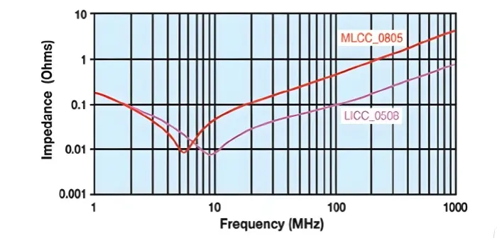
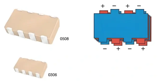
2) Use special lead or electrode designs
Some packages change electrode shapes to reduce loop area. For example, low-inductance chip
capacitors (LICC) place electrodes on a wide side. That shortens the current path and lowers
equivalent series inductance (ESL). An LICC in 0508 size can have a much lower ESL than a
normal 0805 MLCC.
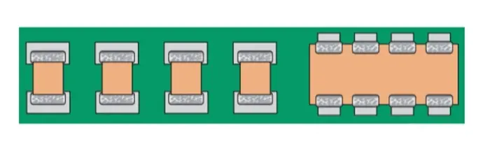
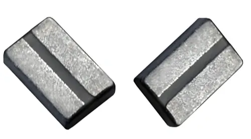
3) Interdigitated capacitors (IDC)
Interdigitated capacitors put fingers of electrodes next to each other. The fingers create
currents that are always in opposite directions and closely located. That cancels the
inductance and lowers ESL.
4) LGA style capacitors
LGA (land grid array) capacitors have multiple pads or electrodes on the bottom. They
combine the ideas of multiple terminals and short current paths. LGA gives low inductance
and makes mounting easy for some board types.
5) Array types and capacitor arrays
Manufacturers also make arrays that combine several capacitors in one package. These arrays place multiple capacitors close together and in multiple terminals. The goal is to give a mix of capacitance and low ESL in a small area.
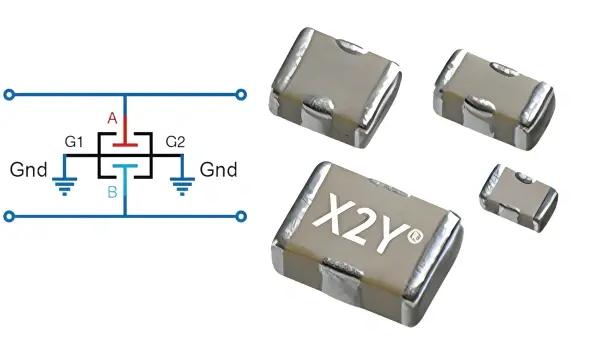
6) X2Y capacitors
X2Y parts are special. They have four terminals. The top and bottom terminals connect to the
power rails. The middle terminals connect to ground. You can see X2Y as four capacitors in
parallel between power and ground. The way the electrodes are placed makes the series
inductance very low. This gives a very small ESL and good high-frequency performance.
Performance Comparison
To give an idea, here are sample ESL numbers (these values can vary with vendor and part, but they show the relative size):
| ESL (pH) | |||||||
|---|---|---|---|---|---|---|---|
| EIA Size | MLCC | EIA Size | LICC | EIA Size | 8T IDC | EIA Size | 2T LGA |
| 1206 | 1000 | 0612 | 170 | 0612 | 60 | ||
| 0805 | 525 | 0508 | 130 | 0508 | 45 | 0805 | 45 |
| 0603 | 450 | 0306 | 110 | 0306 | 35 | 0306 | 35 |
| 0402 | 300 | 0204 | 40 | ||||
| 0201 | 120 | ||||||
You see that IDC and LGA are much lower than a normal MLCC. LICC is lower than MLCC but higher than IDC/LGA. In this example, IDC/LGA ESL is less than one-tenth of the MLCC ESL for the same footprint size. That is a big change.
Practical Design Recommendations
Designers' Checklist
Use these guidelines to select and place capacitors effectively in your PCB designs.
You do not need every new part. Still, you should learn why they exist. Then apply the same rules in your design:
- Use capacitors with low ESL when you need clean power at high frequency.
- Put decoupling capacitors close to power pins. Make the route short and wide.
- Keep the power and return traces close together. Use vias close to the capacitor pads.
- Use multiple capacitors in parallel to cover different frequency ranges. For example, mix bulk caps for low frequency and small MLCCs for high frequency.
- Use plane pairs (power and ground) close to each other to provide distributed capacitance.
- When the highest speed or lowest noise matters, consider low-ESL parts like IDC, LGA, LICC, or X2Y types.
- Every millimeter of trace and every pad counts at high frequency. Treat each trace as part of the PDN, not just a simple wire.
A Capacitor's "Career"
If we view one capacitor as a person, here is its career path:
- Start as a large through-hole ceramic or a big MLCC. It has more inductance.
- Make the package smaller (0603, 0402). Inductance goes down.
- Add more parts in parallel to reduce equivalent inductance.
- Change internal electrode shapes to LICC or IDC style. ESL drops further.
- Move to array or multi-terminal packages like LGA and X2Y for very low ESL and simple layout.
The reason for all that work is clear: modern chips need clean power at ever higher speeds. The capacitor's job is to fight noise. To do that, the capacitor must have very low inductance and must be placed in very short loops on the PCB.
Summary
I explained why many odd-shaped ceramic capacitors exist. The shapes change to lower inductance. Lower inductance helps the capacitor work at high frequency. That keeps PDN impedance low and reduces switching noise. The new package forms use small size, special electrode layouts, multiple terminals, and internal arrays. They let designers meet strict PDN goals without making the board layout too complex.
You will not use every type in every project. Still, the basic rule is simple and always useful:
Choose low-inductance capacitors and make the decoupling loop as short and tight as possible.
If you follow that rule, the power rails will be cleaner. Your high-speed chips will behave better.
Need a PCBA Quote?
Get professional pricing for your PCB assembly project. Our experts can help select the right capacitors for your design requirements.
Request PCBA QuoteExpert component selection advice
Fast turnaround quotes (within 24 hours)
High-frequency design support