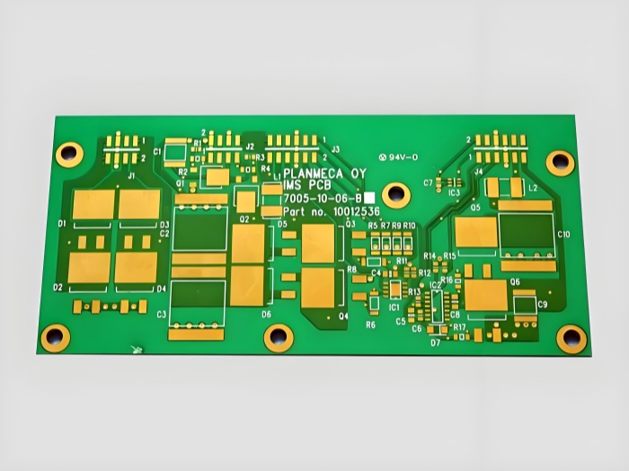
Copper on a circuit board is primarily electrolytic (pure) copper, which readily
oxidizes in air. Oxidation degrades conductivity—leading to poor solder wetting or
contact failures—and thus reduces PCB performance. To prevent this, copper pads receive
a surface finish.
Immersion gold (ENIG) deposits a thin gold layer on
the copper. Gold effectively isolates copper from air and prevents oxidation, so ENIG is
an anti‑oxidation treatment that chemically covers the copper with gold. It is also
called “chemical gold.”

The ENIG process aims to deposit a bright, smooth, solderable nickel‑gold plating on the
PCB surface. It consists of four main stages:
- Pre‑treatment (degreasing, micro‑etch, activation, post‑immersion rinse)
- Nickel plating
- Gold plating
- Post‑treatment (waste‑gold rinse, DI water rinse, drying)
Typical pre‑treatment steps are:
- Degreasing (30 % AD‑482)
- Micro‑etch (60 g/L APS, 2 % H₂SO₄)
- Activation (10 % Act‑354‑2)
- Post‑immersion (1 % H₂SO₄)
These steps remove copper oxides and deposit palladium on the copper to activate the
surface for nickel plating. Any lapse here will compromise subsequent nickel and gold
deposition and may cause batch rejects. Process baths must be regularly analyzed and
replenished within specified ranges. For example, micro‑etch rate should be 25 μ–40 μ;
activation solution must be replaced once copper content exceeds 800 ppm. Weekly tank
changes and cleanings of the degreasing, micro‑etch, activation, and rinse baths are
critical to maintain PCB quality.
Electroless nickel plating requires strict control of bath composition and operating
conditions. The bath should be analyzed twice per shift, and nickel reducer replenished
based on board copper area or experience. Additives must be dosed in small, distributed
increments to avoid local over‑reaction and accelerated aging. Bath temperature strongly
affects nickel thickness—maintain 85 °C–90 °C—and pH should be 5.3–5.7. When not in
production, lower the bath to ~70 °C to slow aging. Electroless nickel is sensitive to
impurities; inhibitors include low‑melting heavy metals (Pb, Sn, Hg, Ti, Bi).
Immersion gold is a displacement (immersion) process. A typical gold bath contains
1.5–3.5 g/L Au and 0.06–0.16 mol/L complexing agent. The bath operates at pH 4–5 and
85 °C–90 °C, producing a smooth, fine‑crystal gold layer by displacing pure gold onto
the nickel‑phosphorus surface.
Post‑treatment steps include:
- Waste‑gold rinse
- DI water rinse
- Drying
If available, a horizontal spray‑rinse system further cleans the board:
- Chemical spray (10 % H₂SO₄ + 30 g/L H₂O₂)
- High‑pressure DI rinse (30–50 psi)
- Final DI rinse
- Blow‑dry and bake
This sequence thoroughly removes residual chemicals and moisture from holes and
surfaces, yielding a uniformly bright ENIG finish.
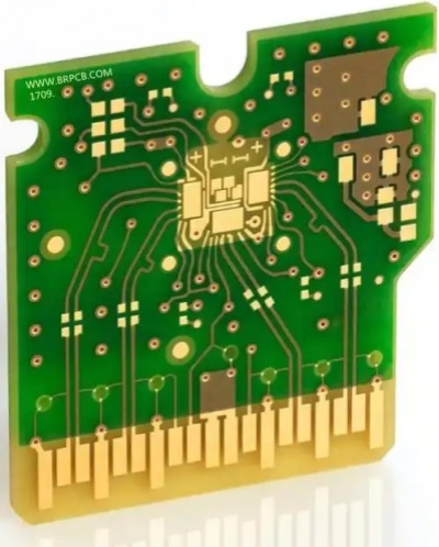
Gold fingers are the brass contact pads on memory modules or edge connectors. They
consist of multiple gold‑plated conductive pads arranged like fingers. All signals
between the module and socket transmit through these “fingers.”

- Stable, bright, smooth plating
- Excellent solderability
- Typical thickness: 1–3 μin
- Four‑stage process (pre‑treat, nickel, gold, post‑treat)
ENIG is more expensive than HASL (hot‑air solder leveling). If gold thickness exceeds
standard fab limits, costs rise further. However, if your design demands high
solderability or electrical performance—such as edge connectors (gold fingers) or fine
line‑space boards—ENIG (plus gold fingers) ensures reliable solder joints, stable
performance, and robust resistance to shock or wear.
For boards with gold‑finger edges but ample trace‑to‑pad spacing elsewhere, you can
specify HASL for the main board and ENIG only on the fingers. This reduces cost while
maintaining edge‑connector reliability. If trace‑pad spacing is tight, HASL may cause
solder bridging and short circuits, and gold fingers suffer from insertion wear and
contact failures.
Select the fabrication process that balances cost control with board performance and
reliability.
- Chemical redox process yields a thick, soft, gold‑colored layer.
- Ideal for high‑density, high‑end applications.
- Applies and levels a solder (tin‑lead or lead‑free) layer with hot‑air knives.
- Most common, low cost, but less planar.
- Solderability: HASL has solder already on the pads, making manual
soldering very easy; ENIG also offers excellent solderability.
- Signal Integrity: ENIG pads bond solder mask and copper more
firmly; signals travel in the copper layer with minimal skin‑effect impact.
- Shelf Life: ENIG resists “black pad” and oxidation, so boards have
longer shelf life; HASL boards oxidize faster.
- Planarity: ENIG is extremely flat; HASL struggles to produce fine,
planar pads, complicating SMT placement.
| Surface Finish |
Solderability |
Cost |
Oxidation Resistance |
Typical Use Case |
| ENIG |
Excellent |
High |
Excellent |
High-density assemblies, high-end devices |
| HASL |
Good |
Low |
Moderate |
General electronics |
| OSP |
Good |
Low |
Moderate |
Eco-friendly consumer electronics |
| Immersion Silver |
Excellent |
Medium |
Moderate |
High-frequency signal products |
- 5G Base Stations: High conductivity and oxidation resistance ensure
stable, low‑loss signal transmission in harsh outdoor environments; dual‑sided ENIG
increases solder yield and extends lifetime.
- Microwave/RF Modules: ENIG meets strict high‑frequency transmission
requirements in satellite ground stations and microwave links.
- Fiber‑Optic Transceivers: Critical electro‑optical conversion
modules rely on ENIG’s electrical stability and corrosion resistance.
- Patient Monitors (ECG, glucose meters): ENIG’s precision
conductivity and stability enable accurate, low‑level bio‑signal capture; corrosion
resistance endures frequent sterilization.
- Imaging Systems (CT, MRI): High‑speed data processing boards
require ENIG for reliable, long‑term performance and reduced imaging errors.
- Avionics: ENIG withstands extreme temperatures, vibration, and
corrosion, ensuring flight‑control and navigation electronics remain reliable.
- Satellite Electronics: In space, ENIG resists cosmic radiation and
thermal cycling, preserving signal integrity and connector reliability.
- Automation Controllers: Harsh factory environments demand ENIG’s
corrosion resistance and electrical stability for sensors and PLCs.
- Smart Monitoring Systems: Real‑time data transmission systems
benefit from ENIG’s high‑speed performance and long‑term reliability, reducing
maintenance costs.
- Smartphones & Tablets: ENIG improves signal integrity and
corrosion resistance in thin, high‑performance boards exposed to moisture.
- Wearables: Compact modules require ENIG for efficient signal
transmission and reliable micro‑component soldering.
 12 Jun 2025 15:18:31 GMT
PCBASAIL
 12 Jun 2025 15:18:31 GMT
PCBASAIL