Ultra-Thick Copper Multilayer PCB Manufacturing Process
 Tue, 15 Jul 2025 02:17:23 GMT
PCBASAIL
Ultra-thick copper multilayer PCBs are integrated connection devices with the function of connecting strong and weak currents. This paper focuses on the manufacturing process of ultra-thick copper multilayer PCBs with a thickness over 0.41 mm. By using a lamination method of single-sided copper-clad laminate + 1.0 mm blackened copper plate + epoxy board + single-sided copper-clad laminate, and non-flowing prepreg for bonding between layers, industry challenges such as white spots and delamination during the lamination of ultra-thick copper have been effectively addressed.
Introduction
Special ultra-thick copper multilayer PCBs first emerged in North America. For example, UPE in Canada initiated the research and production of ultra-thick copper multilayer PCBs in the 1990s and achieved remarkable results. These special boards are applied to components for strong current connection and transmission, as well as in scenarios involving the connection of strong and weak currents. With the rapid development of automotive electronics and power communication modules in China, they have gradually become a type of special PCB with broad market prospects. Market research shows that there is a demand for them in automotive electronics, IGBT assembly, wind power converters, ignition coils, and other fields. Additionally, as printed circuit boards are widely used in the electronics industry, the requirements for their functions are becoming more stringent. Printed circuit boards not only need to provide essential electrical connections and mechanical support for electronic components but are also increasingly being given additional functions. Thus, ultra-thick copper multilayer PCBs, which can integrate power supplies, carry high currents, and offer high reliability, have become new products under research and development in the PCB industry. They have promising prospects, a larger profit margin compared to traditional circuit boards, and significant development value. Ultra-thick copper multilayer PCBs will play a crucial role in the future high-end circuit connection market and are bound to enjoy an even broader market outlook.
Currently, in the industry, the common methods for manufacturing ultra-thick copper printed circuit boards are either the build-up process of successive thickening through electroplating and copper deposition followed by multiple solder mask printing or the use of ultra-thick copper foils. However, the maximum achievable copper thickness by these processes is currently only 0.41 mm (12 oz/ft²). Processing ultra-thick copper multilayer boards beyond this thickness is extremely challenging, and there has been no technological breakthrough in this area yet. The differences between ordinary PCBs and ultra-thick copper PCBs are presented in Table 1. This article mainly explores a new manufacturing process for ultra-thick copper multilayer PCBs. By drawing on the manufacturing process of laminated busbars and adopting the copper plate embedded lamination technology, through process optimization, the manufacturing of ultra-thick copper multilayer printed boards with a thickness exceeding 0.5 mm (14 oz/ft²) has been realized.
Table 1 Differences between Ordinary PCB and Ultra - Thick Copper PCB
| Comparison Points | Ordinary PCB | Ultra-Thick Copper PCB |
|---|---|---|
| Circuit Copper Thickness | ≤0.1mm (3 oz) | >0.5 mm (14 oz) |
| Finished Board Thickness | 1.0 mm - 2.0 mm (mainly 1.6 mm) | 2.0 mm - 3.0 mm (with the inner layer containing copper mainly 1 mm) |
| Connection Method | Mainly welding, no counter - sinking required for installation | Welding, mechanical pre - tightening |
Manufacturing Process of Ultra-Thick Copper Multilayer PCBs
1.1 Lamination Structure
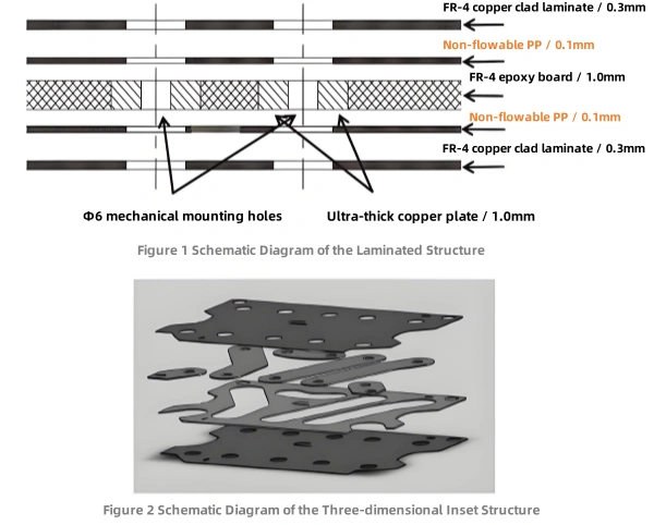
This paper focuses on an ultra-thick copper three-layer board with an inner-layer copper thickness of 1.0 mm, an outer-layer copper thickness of 0.3 mm, and a minimum outer-layer line width and pitch of 0.5 mm. The surface layer consists of a 0.3-mm-thick FR4 copper-clad laminate (glass fiber epoxy resin copper-clad laminate), which undergoes single-sided etching. The bonding layer is a 0.1-mm-thick non-flowing PP sheet (prepreg). The ultra-thick copper plate is embedded in the corresponding hole structure of the FR-4 epoxy board, as shown in Figure 2.

1.2 Processing Flow
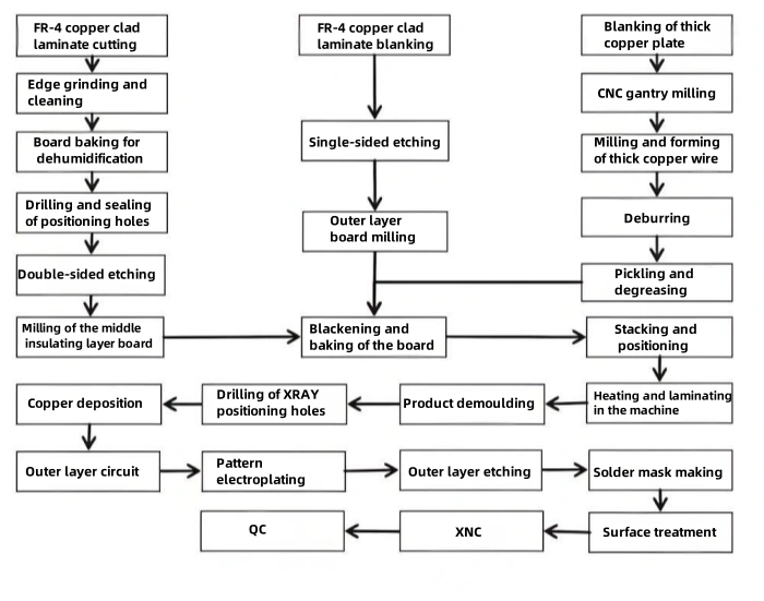
The processing flow of ultra-thick copper PCBs is shown in Figure 3. The main machining operations include milling the surface and middle layers of the board and numerically controlling the milling of the thick copper plate. After surface treatment, the components are stacked and laminated in an integral mold by heating. After demolding, the finished product is fabricated following the conventional PCB processing flow.
 Figure 3 Main Process Flow Chart
1.3 Key Process Methods
1.3.1 Ultra-Thick Copper Inner-Layer Lamination Technology
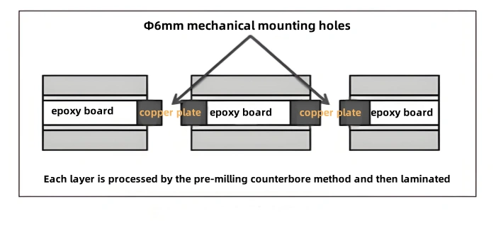
For the inner-layer lamination of ultra-thick copper, it is difficult to reach the required thickness using copper foil. In this study, a 1-mm electrolytic copper plate is employed for the ultra-thick copper inner layer. It is a commonly available material and can be easily procured. The plate is directly processed and formed by a milling machine. The outer contour of the copper plate in the inner layer is fabricated using an FR4 board (glass fiber epoxy resin board) of the same thickness as the overall filling. To facilitate lamination and ensure a close fit around the copper plate, the gap between the two contours is controlled within 0 - 0.2 mm, as illustrated in Figure 4. With the filling of the FR4 board, the issue of ultra-thick copper plate thickness is resolved, and the tight lamination and internal insulation after lamination are guaranteed, enabling the design of an inner-layer copper thickness greater than 0.5 mm.
 Schematic Diagram of Epoxy Board Filling
1.3.2 Ultra-Thick Copper Blackening Technology
Before lamination, the surface of the ultra-thick copper needs to be blackened. Blackening the copper plate can increase the contact surface area between the copper surface and the resin and enhance the wettability of the high-temperature flowing resin to the copper. This allows the resin to penetrate into the gaps of the oxide layer. After hardening, it exhibits strong adhesion, improving the lamination effect. Moreover, it helps to mitigate issues such as white spots during lamination and the whitening and blistering of the board surface after the baking test (287°C ± 6°C). The specific blackening parameters are listed in Table 2.
| Process Name | Control Items | Process Range | Control Standard |
|---|---|---|---|
| Alkaline Degreasing | Temperature (°C) | 60 ± 5 | 60 |
| #402-L (V/V) | (25 ± 3) % | 25% | |
| Roughening | Cu²⁺ (g/L) | ≤30 | ≤30 |
| H₂SO₄ (V/V) | 2% - 4% | 3% | |
| Na₂S₂O₈ (g/L) | 30 - 60 | 45 | |
| Temperature (°C) | 30 ± 5 | 30 | |
| Pre - immersion | E - 501 - B (V/V) | (1 ± 0.5) % | 1% |
| Black Oxidation | E - 501 - A (V/V) | (23 ± 3) % | 23% |
| E - 501 - B (V/V) | (8 ± 1) % | 8% | |
| Temperature (°C) | 80 ± 2 | 80 | |
| Hot Water Washing | Temperature (°C) | 50 ± 5 | 50 |
Table 2 Blackening Process Parameter Table
1.3.3 Ultra-Thick Copper PCB Lamination Technology
Due to manufacturing tolerances in the thickness of the ultra-thick copper plate in the inner layer and the surrounding FR-4 board used for filling, their thicknesses cannot be exactly the same. If the conventional lamination method is adopted, defects such as white spots and delamination are likely to occur during lamination, and the lamination process becomes challenging. To reduce the lamination difficulty of the ultra-thick copper plate layer and ensure dimensional accuracy, through experimental verification, an integral lamination mold structure is utilized. The upper and lower templates of the mold are made of steel, and a silica gel pad serves as the intermediate buffer layer. By setting appropriate lamination temperature, pressure, dwell time, and other process parameters, the desired lamination effect is achieved. This also addresses technical problems such as white spots and delamination during ultra-thick copper lamination, meeting the lamination requirements of ultra-thick copper PCBs.
- Ultra-thick Copper PCB Lamination Method
Due to the low fluidity of non-flowing PP resin, if conventional covering materials like kraft paper are used, the PP sheet cannot be evenly pressed, resulting in defects such as white spots and delamination after lamination. Therefore, a silica gel pad is essential as a key buffer layer during the lamination of thick copper plate PCB products. It plays a role in evenly distributing the pressure during lamination. Additionally, to address the lamination issue, the pressure parameter in the laminator is adjusted from 2.1 Mpa (22 kg/cm²) to 2.94 Mpa (30 kg/cm²), and the temperature is adjusted to the optimal fusion temperature of 170°C according to the characteristics of the PP sheet.
- Ultra-thick Copper PCB Lamination Parameters
The parameters are presented in Table 3.
Step Temperature Pressure Vacuum °C min Mpa (PSI) min Mpa (mm/Hg) min 1 170 20 0.96 (140) 1 0.098 (740) 60 2 170 60 0.96 (140) 19 0.098 (740) 70 3 100 10 1.9 (280) 1 0 0 4 50 10 1.9 (280) 59 0 0 5 30 20 1.9 (280) 30 0 0 6 20 20 1.9 (280) 30 0 0 - Ultra-thick Copper PCB Lamination Effect
After testing in accordance with Section 4.8.5.8.2 of GJB362B - 2009, when inspecting the PCB according to 4.8.2, there should be no blisters and delamination exceeding the allowable limits specified in Section 3.5.1.2.3 (sub-surface defects). The PCB samples meet the appearance and dimensional requirements in 3.5.1. After microsectioning and inspection according to 4.8.3, they comply with the requirements specified in 3.5.2. The sectioning results are shown in Figure 6. From the lamination section, it can be seen that the circuit is fully filled, with no microcracks or bubbles.
 Figure 6 Sectional View of the Lamination Effect
1.3.4 Ultra-Thick Copper PCB Resin Flow Control Technology
Unlike general PCB processing, the outer shape and device connection holes of ultra-thick copper PCBs are completed prior to lamination. Excessive resin flow will affect the roundness and dimensions of the connection parts, failing to meet the appearance and usage requirements. During the development of this process, the process route of laminating first and then milling the outer shape was also tested. However, it requires strict control over the subsequent outer shape milling, especially when processing the connection parts of the inner thick copper layer, where the depth accuracy control is extremely demanding, resulting in a low qualification rate.
Selecting the appropriate bonding material and designing a reasonable device structure is one of the research challenges. To address the issue of resin overflow appearance caused by ordinary prepregs after lamination, a prepreg with low fluidity (Shengyi: SP120N) is used. This bonding material features low resin fluidity, flexibility, excellent heat resistance, and electrical properties. Based on the resin overflow characteristics, the contour of the prepreg in specific positions is adjusted, and a specific shape contour is processed through cutting and plotting. This enables the implementation of the process of forming first and then laminating. After lamination, the outer shape is already formed, eliminating the need for secondary CNC milling of the outer shape. As a result, the resin flow problem after lamination of the PCB is resolved, ensuring that there is no resin flow on the connection surface after lamination of the ultra-thick copper plate and that the lamination is tight.
Ultra-Thick Copper PCB Finished Product Effect
2.1 Performance Tests
2.1.1 Withstand Voltage Test
The poles of the ultra-thick copper PCB samples are subjected to a withstand voltage test. The test voltage is AC1000V for 1 minute, and there is no breakdown or flashover.
2.1.2 High-Current Temperature Rise Test
Corresponding connecting copper plates are designed to connect the poles of the ultra-thick copper PCB samples in series, and they are connected to a high-current generator for testing with specific test currents. The test results are shown in Table 5.From the temperature rise data in Table 5, it can be seen that the overall temperature rise of the ultra-thick copper PCB is relatively low and can meet the actual usage requirements (generally, the temperature rise requirement is below 30 K). The high-current temperature rise of the ultra-thick copper PCB is related to its structure, and different thick copper structures may exhibit certain differences in temperature rise.
2.1.3 Thermal Stress Test
Thermal stress test requirements: In accordance with the General Specification for Rigid Printed Circuit Boards GJB362B - 2009, the samples are subjected to a thermal stress test, and then visually inspected for any defects such as delamination, blistering, pad lifting, and white spots.After the appearance and dimensions of the PCB samples meet the requirements, they need to be microsectioned. However, due to the excessive thickness of the inner thick copper in this sample, metallographic sectioning cannot be performed. Therefore, after the thermal stress test at 287°C ± 6°C, only the appearance of this sample is visually inspected.The test result shows that there are no defects such as delamination, blistering, pad lifting, or white spots.
Conclusion
This paper presents a manufacturing process for ultra-thick copper multilayer PCBs. Through technological innovation and process improvement, the current limitations of ultra-thick copper multilayer PCB copper thickness have been effectively overcome, and common processing technical challenges have been addressed as follows:
The ultra-thick copper inner-layer lamination technology effectively solves the problem of ultra-thick copper material selection. The pre-milling and forming process eliminates the need for etching, avoiding the technical difficulties associated with thick copper plate etching. The FR-4 filling technology ensures the tight lamination and insulation of the inner layer.
The ultra-thick copper PCB lamination technology effectively resolves the issues of white spots and delamination during lamination and provides a new lamination method and solution.
The ultra-thick copper PCB resin flow control technology effectively addresses the problem of resin flow after lamination and ensures the implementation of the process of pre-milling the outer shape and then laminating.