Automatic Optical Inspection (AOI) is an intelligent inspection system used to detect
common defects in soldered printed circuit boards (PCBs) and surface-mount assemblies.
Drawing on optical principles, image-comparison algorithms and statistical modeling
techniques, AOI offers a powerful complement to traditional in-circuit test (ICT) and
functional testing (F/T), especially as PCBs and components grow ever more complex.
As PCB densities increase and component sizes shrink—to 0402, 0201 and beyond—manual
visual inspection becomes neither reliable nor cost‑effective. Likewise, “bed‑of‑nails”
ICT fixtures struggle to physically accommodate probes for tightly packed, fine‑pitch
boards. AOI fills this gap by:
- Boosting ICT/F/T yield
- Reducing manual inspection labor costs
- Lowering fixture‑fabrication expenses
- Preventing ICT bottlenecks in the production line
- Shortening ramp‑up time for new product volumes
- Enabling statistical process control
In practice, integrating AOI before or after reflow soldering helps catch solder‑paste,
component‑placement and solder‑joint defects at the lowest possible cost.
Although each AOI vendor offers its own “secret sauce,” almost all systems operate on
three pillars:
- Optical Imaging
- Digital Image Comparison
- Statistical Model‑Based Learning

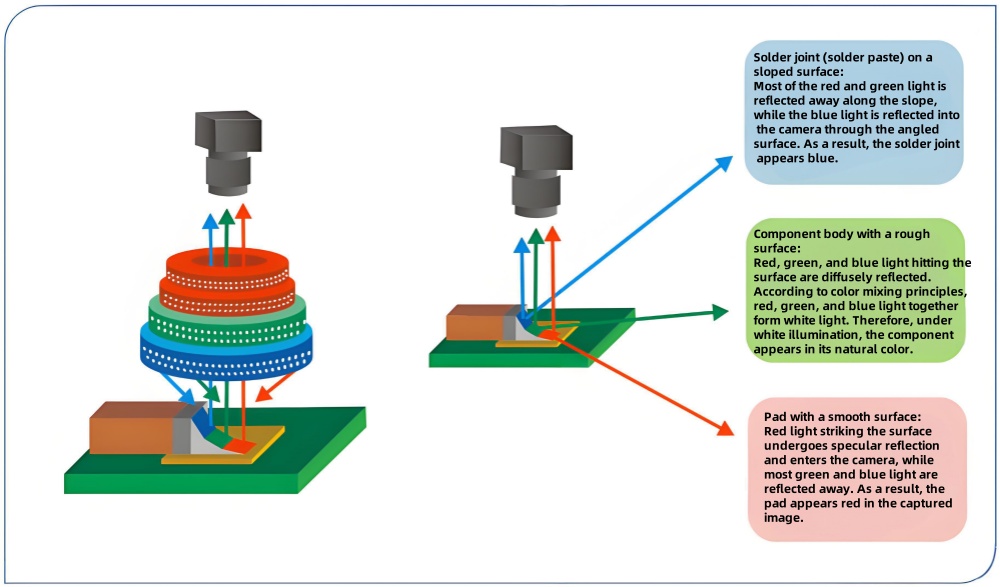
Modern AOI machines employ a tower of red, green and blue LEDs arranged in a 360° ring
around the inspection head. By sequentially illuminating the board with pure R, G, B,
and combined white (RGB) light, the system captures distinct reflections from component
bodies, solder joints and copper pads:
- Copper Pads: Smooth surfaces create specular (“mirror‑like”)
reflections. Under red illumination, they often appear red or yellowish‑white as red
light reflects back most strongly.
- Component Bodies: Rough, diffusive surfaces scatter blue and yellow
light equally, combining into white, so components appear in their true color.
- Solder Joints: The sloped fillet geometry causes yellow light to
scatter outward while blue light reflects into the camera, giving solder joints a
bluish hue.
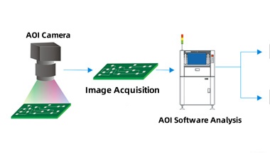
High‑resolution CCD cameras then capture these color‑sequenced images at high speed and
feed them to the processing PC.

Once digitized by the frame grabber, each image is converted into pixel‑level brightness
and color values. AOI software applies one or more mathematical methods—such as template
matching, edge detection, grayscale modeling, feature extraction, vector analysis,
pattern matching or even Fourier transforms—to compute a “deviation score” for every
inspected feature.
- If the deviation stays below a calibrated threshold, the feature passes.
- If it exceeds that threshold, the feature is flagged as defective.
By adjusting thresholds and combining multiple algorithms, the system can be tuned for
specific components, pitches and board layouts.

AOI depends on a “golden board” or on a library of pre‑approved images. During setup,
the machine either learns from a sequence of known‑good boards or imports ideal images
from a database. Through statistical modeling, AOI derives the acceptable range of
variation for each component’s shape, color distribution and placement pattern. This
multivariate “OK‑model” guides future inspections, automatically accommodating minor,
permissible variations in manufacturing.
The machine continuously monitors LED output levels—affected by temperature drift or LED
aging—and automatically adjusts drive current (“auto‑tracking”) to maintain stable
illumination.
Standard AOI provides high‑accuracy 2D checks of planar features (e.g., pad coverage,
component footprint). Height or coplanarity measurements may require auxiliary sensors
or 3D‑AOI extensions.
Top lights reveal component outlines; bottom (through‑hole) lights highlight solder
fillets. By comparing images under both lighting conditions, AOI discriminates missing
or malformed joints versus correctly soldered ones.
Inspection programs can be generated automatically from Gerber files or manually
created. Users map each component, set acceptable thresholds, and choose relevant
algorithms.
Many AOI systems include OCR to verify component markings, part numbers and polarity
indicators.
During manufacturing, the AOI workflow typically follows these steps:
- Scan a known‑good board to build or verify the inspection program.
- Index production boards through the AOI station.
- Compare each image against the golden model in real time.
- Log and/or mark defects for rework.
AOI can be placed at several key points on a surface‑mount assembly line:
- Post‑Paste Inspection (PPI): Catches solder‑paste volume, offset,
bridge and low‑paste defects immediately after stencil printing.
- Pre‑Reflow Inspection: Verifies component presence, orientation,
offset and polarity before soldering.
- Post‑Reflow Inspection: Detects solder‑joint defects after reflow,
including tombstoning, insufficient fillet, opens, shorts and solder balls.
By locating AOI early—after printing and component placement—the manufacturer can
correct errors when rework costs are lowest. A line‑end (post‑reflow) AOI provides a
final check but comes with higher rework costs, since boards must be removed from the
line for correction.
Industry studies show that over 60% of soldering defects originate from paste‑printing
errors. By installing AOI immediately after printing, manufacturers can eliminate many
defects before they propagate downstream. Likewise, a pre‑reflow AOI station can prevent
misaligned or missing components from entering the oven, saving on both scrap and
downstream testing time.
AOI’s rapid, non‑contact approach delivers consistent, programmable inspection that
scales easily with production volume. When combined with traditional ICT and functional
testing, it provides a comprehensive quality‑control package that keeps modern SMT lines
running smoothly.
Automatic Optical Inspection harnesses advanced optics, high-speed imaging and powerful
algorithms to bring consistency and efficiency to surface-mount assembly quality
control. As boards become more densely packed and components ever smaller, AOI is no
longer a luxury but a necessity—to maintain yields, reduce costs, and ensure reliable
products in today’s high‑technology marketplace.
 Tue, 15 Jul 2025 09:41:36 GMT
PCBASAIL
