- The welding process dimensions for PCB board shape are width (200mm–250mm) × length
(250mm–300mm).
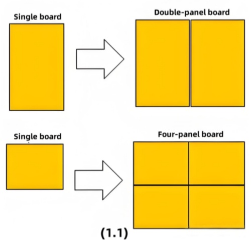
- For PCBs with a long side shorter than 125mm or a short side shorter than 100mm, a
panelization method can be adopted (as shown in Figure 1.1).
- This size helps avoid issues during wave soldering and reflow soldering processes.
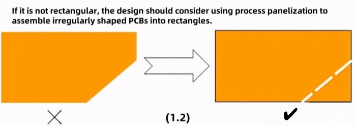
- If the shape is not rectangular, problems such as unstable conveying on the conveyor
belt during welding, board flipping during component insertion, and solder splashing
onto the component side when passing through the wave soldering tin bath may occur.

- For non-rectangular PCBs, process panelization should be used to assemble
irregularly shaped PCBs into rectangles.
- In particular, if there are notches at the four corners, they should be filled to
form a rectangle.
- For PCBs with only surface-mounted components, notches are allowed, but the notch
size must be smaller than 1/3 of the side length where it is located.
In circuit board design, requirements for PCB materials must be specified and noted in
the technical requirements of the circuit board design documents, including:
- PCB material and grade (commonly epoxy glass fiber cloth base FR-4, FR-5);
- Flammability rating (UL94-V0, UL94-V1, or green flame-retardant type);
- Board thickness, nominal specifications: 0.8, 1.0, 1.2, 1.6, 2.0, 2.5, 3.0, 3.5
(unit: mm);
- Board thickness tolerance: ±10%;
- For medical device products, the board thickness must be ≥1.6mm, grade A1 or A2;

PCB plating types include tin plating (preferred) and nickel-gold plating. Tin-plated
PCBs are prone to oxidation when exposed to air for a long time, so vacuum packaging is
recommended for factory storage.
Multilayer PCBs have outstanding effects in electromagnetic compatibility (EMC)
protection but also have higher manufacturing costs. During design, a compromise should
be made based on signal requirements.
- For fclk>5MHz
or tr<5ns (pulse rise or
fall time), multilayer boards are recommended;
- After deciding to use multilayer boards, the number of routing layers should be
determined based on pin density.
- If a double-layer board must be used, one side of the printed board should be used
as a complete ground layer.
During PCB design, sufficient space and reference points must be reserved for the
production process to avoid technical hazards.
- During the assembly and welding process, the conveying sides of the PCB should each
have a blank width of ≥5–10mm without components or solder joints, serving as
process edges.
- If the PCB cannot have process edges, auxiliary edges of 5–10mm can be added to both
conveying sides as process edges, which will be broken off after welding.
- The PCB must have reference points (also called optical MARK points) for assembly,
serving as alignment references for component placement. The pad shape and
symmetrical layout of the reference points should be determined in consultation with
the assembly manufacturer’s process engineers.
- A background area should be set around the MARK points, where no other pads,
silkscreen, or solder mask are allowed.
The quality of pads directly affects soldering results, so pad design is crucial.
- Ideal soldering conditions with good wetting angles are achieved when the pad hole
diameter is 0.3–0.5mm wider than the component lead diameter, and the total pad
diameter is 2–2.5 times the pad hole diameter.
- For through-hole resistors, capacitors, inductors, beads, diodes, and transistors,
the through-tin pad hole diameter D = component
lead outer diameter d
+ (0.3–0.5mm).
- The pads at both ends of surface-mount pads should be well symmetrical to ensure
balance of molten solder surface tension and avoid bridging or displacement during
soldering; violating this requirement can easily cause soldering defects during
reflow soldering.
Via design rules: Standard via dimensions are:
- Hole diameter: board thickness ≥ (1:6)
- For high-speed signals, one via generates 1–4nH inductance and 0.3–0.8pF
capacitance. When routing high-speed signals, vias should be minimized; for parallel
high-speed signal lines (e.g., address and data lines), if layer changes are
unavoidable, ensure the number of vias is the same for all parallel signal lines.
- Through-hole components with multiple pins on the soldering side (e.g., connectors,
DIP packages, T220 packages) should be laid out with their axes perpendicular to the
wave soldering direction.
- Active components such as PLCC and QFP should avoid wave soldering.
- The same type of through-hole components should be placed in the same direction in
the X or Y axis;
Recommended minimum spacing between components:
- SMD resistor/capacitor pad edges: >0.3–0.7mm;
- Between other chip components, SOTs, SOIC and chip components: 1–1.25mm;
- Between SOICs, SOIC and QFP: 1.5–2.0mm;
- Between PLCC and chip components, SOIC and QFP: 2–2.5mm;
- Between PLCCs: 3–4mm;
- Between through-hole component pad outer edges and chip component pad outer edges:
>1.5–2mm;

The relationship between PCB copper trace width/thickness and current-carrying capacity
is determined according to industry standards.
- Current passing through printed traces causes temperature rise, which is related to
trace width when copper thickness is constant. If increasing trace current is
required but widening is impossible, trace temperature rise must be fully evaluated.
- Gold fingers protruding from the board edge, both ends of the board side with gold
fingers (rounded corners R1.0–R1.5), and the plugging end face of gold fingers
should be chamfered;
- No pads should be on the inner end of gold fingers, and pads/components should be
kept away from gold fingers.
- A/D signals, input/output signals, large/small currents, high/low voltages, and
high/low frequency signals must be kept apart; if separation is impossible, ground
planes should be laid between them for isolation.
The following areas and content on the PCB should be silk-screened: PCB version number,
pin symbols, component polarity, component orientation, safety markings, and parameter
values at key points (e.g., supply voltage labeled next to power sockets).

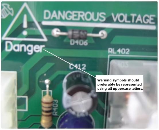
- Warning labels should use all uppercase letters, while explanatory text should start
with uppercase and follow with lowercase letters.
- Silk-screen labels should be placed next to corresponding components, not covered by
installed component bodies, and maintain consistent orientation within each single
board.
- No silk-screen should be on pads, solder tracks, vias, or test pads.
- Silk-screen should clearly indicate representative pin numbers to facilitate
identification of other pins.
- ICT test points on the PCB should be on the soldering side; test pad size ≥24mil
(0.6mm); minimum spacing between two separate test points 60mils (1.5mm);
- For single boards requiring ICT testing, two non-metallized holes should be designed
at the diagonals for ICT test positioning;
- SMT component pads should not double as test pads.
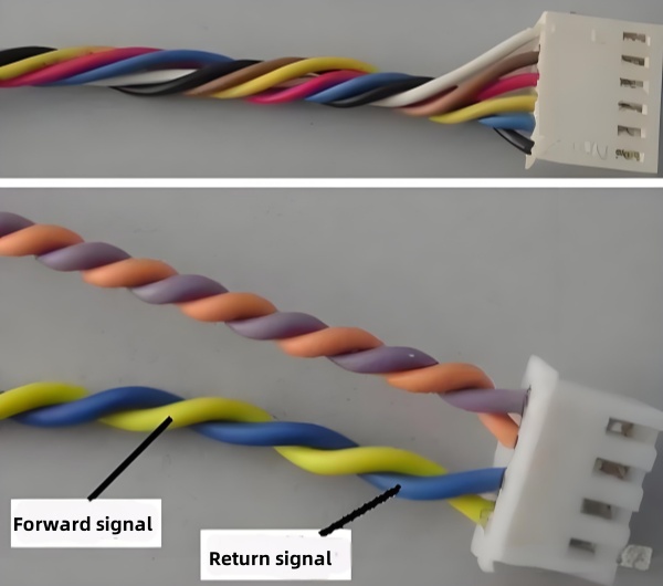
Unshielded Signal Wire Twisting Guidelines:
- For unshielded signal cables, incompatible signal wires (in/out, A/D signals,
high/low voltage signals, high/low frequency signals) should not be twisted
together;
- Signal forward and return paths should be twisted with each other.

- For signals above 10MHz, use multi-point grounding nearby with large-area ground
plane copper pouring.
- Grounding rules for mixed high/low frequency circuits:
- ≤1MHz: single-point grounding (but note common impedance interference);
- ≥10MHz: multi-point nearby grounding;
- 1–10MHz: single-point grounding if ground wire length <λ/20, multi-point
nearby grounding if ground wire length >λ/20 (λ = wavelength).
 30 May 2025 14:55:50 GMT
PCBASAIL
