Next‑Gen Mixed‑Assembly Soldering for Complex PCBs
 Wed, 16 Jul 2025 01:08:55 GMT
PCBASAIL
Table of Contents
In traditional electronics‐assembly processes, wave soldering has been the go‑to method
for soldering printed circuit boards (PCBs) that carry plated‑through hole (PTH)
components. But wave soldering isn’t without its flaws: you can’t use it on boards that
have high‑density, fine‑pitch surface‑mount devices (SMDs); it’s prone to solder
bridging and misses; it requires flux spraying; and the board itself takes a hefty
thermal shock, often warping or distorting. Nowadays, circuit assemblies are getting
denser and denser, and you inevitably end up with fine‑pitch SMDs right next to your PTH
parts. Wave soldering just can’t keep up. The usual workaround is to reflow only the
SMDs first, then manually touch‑up the remaining PTH joints—but that leads to
inconsistent joint quality.

To tackle these challenges, several hybrid soldering techniques have emerged: selective
soldering, through‑hole reflow (THR), and masked wave soldering, just to name a few.
These methods shield the delicate SMDs while you solder the PTH parts, slashing both the
number of production steps and the total cycle time. What follows is a rundown of these
hybrid processes.
1. Overview of Hybrid Soldering Technologies
1.1 Selective Soldering
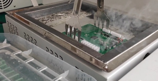
You can really appreciate selective soldering if you compare it side‑by‑side with wave
soldering. The biggest difference is this: with wave soldering, you dunk the entire
underside of the PCB into molten solder, whereas in selective soldering, only specific
zones ever touch the solder wave. Since a PCB is such a lousy conductor, the nearby
components and pads don’t get enough heat to reflow unintentionally.
Just like wave soldering, you still need to pre‑apply flux. But instead of spraying the
whole board, you only coat the individual areas you plan to solder. Note that selective
soldering isn’t made for SMDs—it’s purely for PTH joints.
There are two main flavors of selective soldering:
(1) Drag‑Solder Process
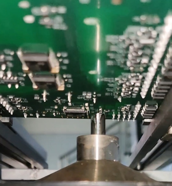
In drag soldering, a single small nozzle creates a mini solder wave (see Figure 1). Drag
soldering is great when you have just a handful of joints or a tight cluster of pins to
solder. The PCB is moved past the solder nozzle at specific speeds and angles to nail
each joint. To keep things stable, that nozzle’s diameter is under 6 mm. Once you set
the solder flow direction, you can orient and optimize the nozzle however you need. A
robot arm can approach the solder wave at angles anywhere between 0° and 12°, but most
folks find a 10° tilt gives the best results.

Because both the solder wave and board are moving in drag soldering, heat transfer is
more efficient than in dip soldering. But since each joint depends on that tiny solder
wave, you need higher solder temperatures—typically around 275–300 °C—and a drag speed
of about 10–25 mm/s. People also flood the solder zone with nitrogen to prevent
oxidation, which in turn reduces bridging defects and boosts process stability and
reliability.
These machines are built for precision and flexibility. The modular design means you can
customize them to your unique production needs—and upgrade later as volumes grow. One
robot arm can handle flux spraying, pre‑heat, and soldering, all in one setup, thanks to
a synchronized process flow that shrinks cycle times. The arm’s precise positioning
(±0.05 mm) ensures each board is treated exactly the same way. And because it can move
in five axes (X, Y, Z, plus U and θ), you can hit joints from any angle for top‑notch
quality. There’s even a titanium probe that regularly measures the solder wave
height—and feeds back to the pump speed—to keep everything rock‑solid.
But drag soldering has its downside: it’s time‑intensive. Between fluxing, pre‑heating,
and soldering, each joint is handled one at a time. More joints means more time—so drag
soldering can’t match wave soldering’s sheer throughput. That’s changing, though, with
multi‑nozzle heads. A dual‑nozzle drag setup can double your output, and you can even
add a second flux nozzle to match.
(2) Dip‑Solder Process
Dip soldering uses multiple solder nozzles—one for each PTH joint—so it trades off some
of drag soldering’s flexibility for higher throughput that rivals wave soldering. It’s
also less expensive to set up. Depending on board size, you can do single or multiple
boards in parallel, with each board getting fluxed, pre‑heated, and soldered all at
once.
Because each board’s joint layout is unique, you need a custom nozzle array for each
board. These nozzles are as large as possible to ensure process stability without
disturbing nearby parts. That design work is crucial—and tricky—because a stable process
often hinges on having just the right nozzle dimensions.

Dip soldering can handle joint sizes from 0.7 to 10 mm, including short leads and small
pads, with low bridging risk—just make sure there's at least 5 mm clearance between
nozzles, components, and pad edges. Typical process settings:
1.2 Through‑Hole Reflow (THR)
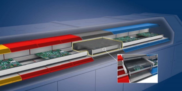
In simple terms, Through‑Hole Reflow (THR) uses reflow soldering to assemble both PTH
and odd‑shaped components in one go. As miniaturization, added features, and higher
component density become critical, most single‑ and double‑sided boards are SMD‑heavy.
Yet PTH parts—especially edge connectors—still have the edge in strength, reliability,
and compatibility.
Traditionally, you’d fit SMDs via stencil and reflow, then wave solder or hand‑solder
the PTH parts. But with THR, you stencil both SMD and PTH pads in one shot, place all
parts, then reflow everything together . For boards with mostly SMDs and only a few PTH
parts—think motherboards with connectors, discrete semiconductors, switches, jacks—you
can skip wave soldering altogether.
1.2.1 Solder‑Paste Application for THR
THR typically needs about 30× more solder paste for each PTH joint versus an SMD pad.
There are two main ways to deposit that extra paste:
By using THR, you not only protect your SMDs, you also dramatically improve through‑hole
joint quality—often making up for the higher equipment cost.
1.2.2 Component Placement for THR
High‑profile or oddly shaped PTH parts—like tall connectors or heavy switches—demand
special handling. Your pick‑and‑place needs:
Modern machines—like Advantis AX72 or Polaris—handle taped, tube, and waffle‑pack PTH
parts right on the same head they use for SMDs. They’re fast, accurate, and reliable.
Manual insertion is a backup for big pin‑count connectors—low cost but slower and less
precise.
1.2.3 THR Reflow Profile
Reflow profiles for THR must deliver enough heat to every pin—all the way up those tall,
heavy connectors. IR reflow ovens are the norm, since hot‑air convection can cause
temperature swings. Split‑zone top/bottom heating helps manage the delta T across the
board. For a heavy 25‑pin D‑SUB, you might raise the bottom heater temp and lower the
top to get the board body hot enough without overheating the connector shell. You also
stretch the time above liquidus so flux has time to boil off from the hole.
Cross‑section analysis is key to validate your profile. Always monitor peak
temperatures, ramp rates, time above liquidus, and cooling rate to avoid voids, thermal
shock, and excessive gradients.
1.3 Masked Wave Soldering
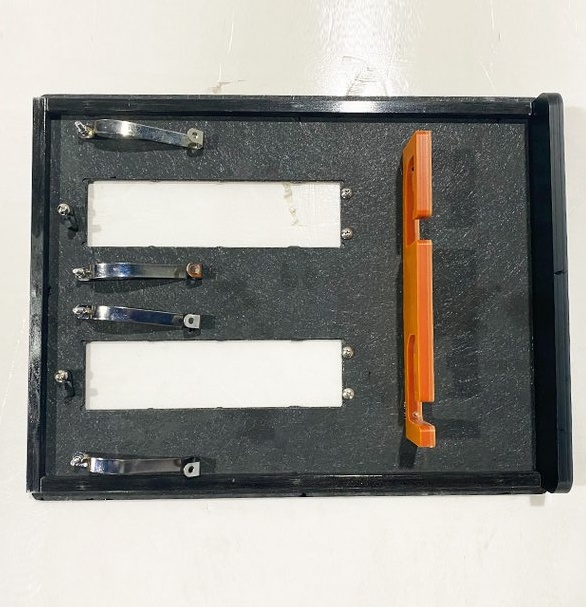
Since wave soldering can’t handle fine‑pitch SMDs, masked (or shielded) wave soldering
steps in: you slip a custom mask—or “shadow” fixture—over the board, covering the SMDs
so only the PTH leads are exposed.

1.3.1 Advantages of Masked Wave
1.3.2 Mask Materials
Must be ESD‑safe: aluminum, synthetic stone (domestic or imported), or fiberboard. Avoid
black stone—it can foul the wave sensors.
Thickness: pick 5–8 mm based on the tallest backside component.
1.3.3 Fixture Design Guidelines
2. Conclusion
As PCB assemblies get more complex, wave soldering alone can’t cut it—especially when
you have fine‑pitch, high‑density SMDs on your solder side. Manual PTH soldering breeds
inconsistent quality. The answer is hybrid soldering: selective soldering, THR, or
masked wave. Which you choose depends on your product mix and volumes:
Both are easy to control and are already widespread. THR is a bit tougher to nail down
but offers the best joint quality, process simplification, and future growth potential.
With assembly densities set to keep climbing, these hybrid technologies will only matter
more—and give PCB designers fresh process options.