Introduction to PCB Surface Finishing Processes
 13 May 2025 13:36:53 GMT
PCBASAIL
Table of Contents
Requirements for PCB Surface Coating in SMT Assembly
Surface Coating Types
Common surface coating types include electroless Ni/Au, electroless Ag, electroless Sn,
OSP (Organic Solderability Preservative), and lead-free hot air leveling (spray
soldering). These coating methods require ensuring a flat and smooth surface, free of
oxidation and dirt, and with a distinct color difference from the surrounding area.
Appearance Requirements
The surface coating layer needs to be smooth and flat, free of oxidation and dirt, and
with a clear color difference from the surrounding area. In addition, the surface
coating layer needs to pass the 3M tape test to ensure that it will not blister,
discolor, or peel off during the SMT assembly process.
Thickness Requirements
The thickness of the surface coating layer needs to meet the standards to ensure that
the solder joints are wet and firm during reflow soldering and wave soldering, avoiding
cold soldering and poor soldering.
Cleanliness Requirements
After being immersed in liquid for 5 minutes, the surface should not have any adverse
reactions and should have good stamping performance.
Environmental Requirements
The surface coating layer needs to meet environmental standards, such as the ROHS
standard, to ensure that the content of lead (Pb≤1000ppm) and other harmful substances
is within the allowable range.
Storage and Transportation Requirements
During storage and transportation, the PCB needs to be maintained under certain
temperature and humidity conditions to prevent the coating layer from getting damp or
damaged. It is generally recommended that the storage conditions are <35°C and the
relative humidity is <75%, and the optimal conditions are <25°C and the relative
humidity is <65%. Humidity control and a non-corrosive gas environment are required.
Lead-Free of PCB
ROHS Ban
Six substances are prohibited: Pb, Hg, Cr⁶⁺ (hexavalent chromium), PBB (polybrominated
biphenyl), PBDE (polybrominated diphenyl ether), and lead is one of them.
Toxicity of Lead
It can cause a decline in intelligence, insomnia, nightmares, weakness, abdominal pain,
headache, and loss of appetite. Typical harmful effects include anemia and disorders of
the central nervous system.
What is Lead-Free?
When the Pb content in the substance is ≤1000ppm, that is, 0.1%, it is lead-free.
What the PCB factory should include to prove to customers that the produced PCB is lead-free:
- The used board material complies with ROHS.
- The solder mask ink complies with ROHS.
- The surface coating is lead-free, such as electroless Ni/Au, electroless Ag, electroless Sn, OSP, and lead-free hot air leveling (spray soldering).
- The produced PCB has been tested and complies with ROHS.
Traditional Surface Treatment Methods:
5.1 Hot Air Leveling of Lead-Tin: Pb:Sn = 37:63, and its lowest melting point is 183°C;
the commonly used solder is Pb:Sn = 40:60, and the melting temperature is 190°C.
5.2 Hot-Melt Lead-Tin: The circuit, pads, and holes are plated with lead-tin (Pb:Sn =
40:60), and then hot-melted in a glycerol bath. The sides of the circuit are also
protected without exposing the copper. Many military products still use this method.
5.3 Pattern Plating of Ni/Au: The board is plated with Ni/Au on the pattern circuit, and
the nickel-gold is used as the anti-corrosion layer. After etching the pattern, the
circuit, holes, and pads are covered with Ni/Au. However, the gold plating on the
pattern circuit and the board edge is wasteful, and it is difficult to ensure the
adhesion of the solder mask printed on the gold surface. Currently, few products use
this method.
Formulas of Lead-Free Solders:
- US Fusion Welding: 95.9 Sn-3.9 Ag-0.6Cu
- Wave Soldering: 99.3 Sn-0.7 Cu
- EU: 95.5 Sn-3.8 Ag-0.7 Cu
- Japan: 96.5 Sn-3.0 Ag-0.5 Cu, that is, the 305 formula (3.0% silver, 0.5% copper, and the rest is tin, called 305).
For the above formulas, the eutectic point is 217°C, which is 34°C higher than the
melting point of the traditional lead-tin alloy (183°C).
The temperature of the lead-free spray soldering process is 265-270°C.
When performing lead-free spray soldering in the PCB factory, during the production
process, the Cu in the production board and the Cu in the solder continuously dissolve
in the tin furnace to contaminate the tin tank. When spray soldering, it co-melts with
the tin on the welding PAD of the PCB, resulting in poor fluidity of the tin surface and
unsatisfactory tin dispersion during SMT assembly. Therefore, it is necessary to monitor
the Cu content during PCB spray soldering.
PCB Surface Treatment Methods
Lead-Free Spray Soldering
- Process: Micro-etching - Water Washing - Coating with
High-Temperature Resistant Flux - Spray Soldering - Water Washing. (Some factories
preheat the PCB board before micro-etching).
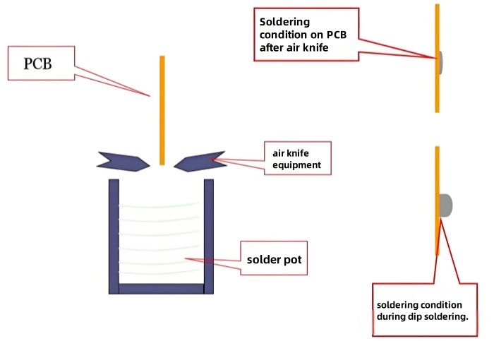
When spraying solder on the PCB, immerse it in the molten lead-free solder (about 265°C), quickly lift the PCB, and use a hot air knife (temperature 300-380°C) to blow the liquid solder flat from the front and back of the board to flatten the meniscus solder on the copper surface and prevent solder bridging. - Equipment: Horizontal and vertical lead-free hot leveling machines. (The coating obtained by the horizontal type is more uniform and suitable for automated production).
- Materials: Lead-free solders, such as SnCuNi, SnCuCo, SnCuGe, or 305 solder. High-temperature resistant flux.
- Requirements: The surface of the pad is 2-5 microns, and the inside of the hole should be less than 25 microns (it can also be relaxed to 38 microns).
- Characteristics: The coating layer is not flat enough, mainly suitable for boards with wide lines and large pads. HDI boards usually do not use this method. It has high requirements for the heat resistance of the copper-clad laminate. The spray soldering process is relatively dirty, has an odor, and is easy to cause burns during high-temperature operation. Its use is limited to a certain extent.
Schematic Diagram of Spray Soldering


OSP (Organic Solderability Preservative)
OSP is also known as preflux (heat-resistant preflux), which is the continuation and
development of the early rosin-based flux.
- Process: Degreasing - Micro-etching - Pickling - Pure Water Washing - OSP - Cleaning - Drying.
- Five Generations of Products: ⑴ Imidazole (or benzotriazole) types;
⑵ Alkyl imidazole types; ⑶ Benzimidazole types; ⑷ Alkyl benzimidazole types; ⑸ Alkyl
phenyl imidazole types.
- The Fourth Generation: Currently, the most used one is alkyl benzimidazole, with a thermal decomposition temperature of 250-270°C, suitable for multiple reflow soldering temperatures under the lead-free soldering temperature (250-270°C).
- The Fifth Generation: Alkyl-phenyl-imidazole type HT-OSP. The decomposition temperature is 354°C, with good thermal stability. It is not easy to form microbubbles and microvoids at the welding interface, improving the welding bonding force.
- Principle: A layer of organic film is formed on the copper surface, firmly protecting the fresh copper surface and preventing oxidation and contamination even at high temperatures. The thickness of the OSP is 0.1-0.2 microns, or 0.2-0.5 microns.
- Characteristics: The process is simple and the cost is low. It can be used on PCBs with low technical content as well as on high-density chip packaging substrates. It is the most promising surface coating process. (Controversy: It is difficult to distinguish colors during assembly. OSP has a similar color to copper. Scratching the board will affect welding. The storage period of OSP is about 6 months).
Currently, OSP can withstand thermal stress (288°C, 10s) three times without oxidation
or discoloration.
Electroless Tin
- Process: Degreasing - Micro-etching - Pickling - Pure Water Washing - Electroless Tin Plating - Cleaning.
- Characteristics: Since all current solders are mainly based on tin, the tin layer can be compatible with any type of solder. From this perspective, electroless tin plating has good development prospects among several types of PCB surface coatings.
- Thickness: 1.0±0.2 microns.
- Problems: ⑴ It cannot withstand multiple soldering operations. The interfacial compound formed after one soldering will become a non-solderable surface. ⑵ Tin whiskers will be generated, affecting reliability. ⑶ The electroless tin solution is likely to attack the solder mask, causing the mask to dissolve and discolor and corrode the copper layer in reverse. ⑷ The electroless tin temperature is high, ≥60°C, and it takes ten minutes to deposit a 1-micron tin layer.
- Improvement: Adding organic additives to the electroless tin solution makes the tin layer structure granular, overcoming the problems of tin whiskers and tin migration, and having good thermal stability.
- Use: Some customers specify the use of electroless tin plating, which is flatter than the lead-free spray soldering layer. It is suitable for communication motherboards. The board after electroless tin plating should be stored in a good room and used within the storage validity period.
Electroless Silver
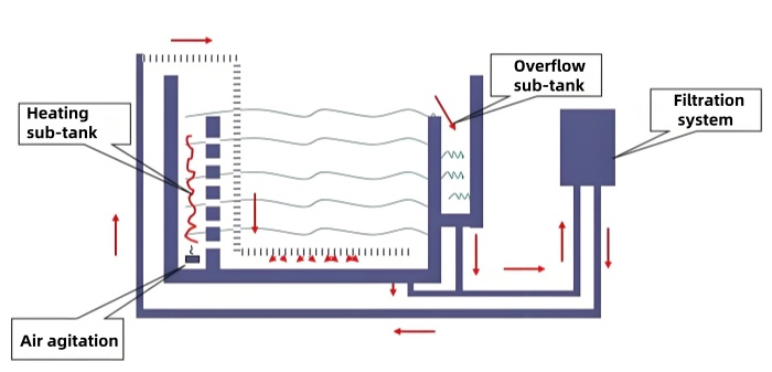
- Process: Degreasing (defatting) - Micro-etching - Pickling - Pure
Water Washing - Electroless Silver Plating - Cleaning.

- Characteristics: ⑴ The process is simple, fast, and the cost is not high. ⑵ The electroless Ag solution contains some organic substances to prevent the silver layer from discoloring and silver migration. ⑶ The thickness of the coating is 0.1-0.5 microns (usually 0.1-0.2 microns), and the welding performance is excellent. ⑷ The silver layer has good inspectability (silver white) during assembly.
- Problems:
The whole line on the Ag immersion production line uses pure water to prevent the silver layer from turning yellow and black. (There are chloride ions in tap water, Ag+Cl → AgCl, generating white precipitation).
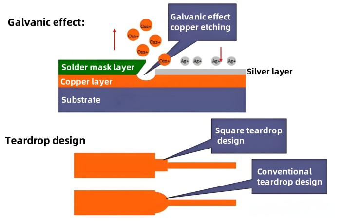
The galvanic effect is likely to occur during electroless silver plating. Therefore, a teardrop design should be added to the circuit design of the electroless silver plate to prevent open circuits.
Silver easily combines with sulfur in the air to form silver sulfide, which is yellow or black.
For all operations, storage, and packaging, sulfur-free gloves should be worn, and sulfur-free paper should be used for packaging. The storage environment has high requirements. It is not allowed to use ordinary paper to separate the boards, and it is not allowed to use rubber bands to wrap the boards.
To prevent silver ion migration, the electroless silver plate should not be stored in a humid environment. Use it within the storage period.
Galvanic Effect of Electroless Silver
Electroplating of Nickel and Gold
- Process: Degreasing - Micro-etching - Pickling - Pure Water Washing - Nickel Plating - Pure Water Washing - Gold Plating (Flash Gold Plating - Thickening Gold Plating) - Gold Recovery - Water Washing.
- Coating Types:
- Hard Gold Plating:
- Used in: PCB plug gold fingers, buttons.
- Characteristics: · Wear-resistant, with good contact and hardness (120-190㎏/㎜²﹚ · Nickel is used as the base, and the thickness of the Ni layer is 3-5 microns; the thickness of the gold layer: 0.1, 0.25, 0.5, 0.8, 1.0… microns. · The gold coating contains cobalt (Co, 0.5%﹚, or metals such as Ni and antimony.
- Soft Gold Plating: Pure gold, 24K gold.
- Purpose: For welding, bonding, etc.
- Characteristics: · Nickel is used as the base, ≥2.5 microns, to prevent the gold layer from diffusing into the copper layer. The nickel layer firmly combines with the solder during welding. The thickness of the Au plating layer is very thin, 0.05-0.1 microns.
- Hard Gold Plating:
- Disadvantages: Gold needs to be plated on the circuit, which is costly. Currently, it is rarely used. The solder mask printed on the gold surface is likely to fall off. The gold layer will become brittle during welding. (When the gold content in the solder is ≥3%)
Electroless Nickel and Immersion Gold (ENIG)
English Full Name: Electroless Nickel and Immersion Gold. Abbreviated as ENIG.
Electroless nickel and immersion gold.
- Process: Degreasing (defatting) - Micro-etching - Post-Micro-etching Immersion - Pre-immersion - Activation - Post-Activation Immersion - Electroless Nickel Plating - Electroless Gold Plating - Cleaning.
- Characteristics:
The electroless Ni/Au coating has a uniform thickness, good coplanarity, good solderability, excellent corrosion resistance, and wear resistance.
It is widely used in mobile phones, computers, and other fields.
The thickness of the nickel layer is 3-5 microns, aiming to prevent mutual diffusion between the copper-gold interface and ensure reliable soldering of the solder joints.
The thickness of the immersion gold layer is usually 0.05-0.15 microns. - Reaction Mechanism:
- Electroless Nickel Plating: Under the catalysis of metal palladium on the copper surface, the electroless nickel plating reaction starts through the reducing agent and nickel ions in the solution. Nickel itself is a catalyst for further electroless nickel plating. Under the action of the reducing agent sodium hypophosphite in the solution, the electroless nickel plating process will continue until the product is taken out of the bath solution. Phosphorus is co-deposited into the coating together with nickel during the deposition process. In fact, electroless nickel plating is the deposition of nickel-phosphorus alloy.
- Immersion Gold: Oxidation-reduction reaction. Gold is deposited on the nickel surface through the nickel-gold displacement reaction.
- Process Instructions:
- Degreasing: Remove the copper oxide layer, oil stains, and fingerprints on the pads to be electroless nickel and gold plated to ensure a good bond between the electroless nickel layer and the copper surface and avoid appearance defects such as stains after immersion gold plating.
- Micro-etching: Further remove the copper surface oxide layer and micro-roughen the copper surface to achieve a good bonding force between the electroless nickel layer and the copper layer.
- Post-Micro-etching Immersion: Neutralize the micro-etching solution in the small holes plugged with green oil, lower the electrode potential, and prevent the situation of missing plating at the connected pad position.
- Pre-immersion: Initially activate the copper surface and prevent the contamination of the activation solution by the previous process to promote the adsorption of the activator on the copper surface.
- Activation: Uniformly replace a very thin layer of palladium on the copper surface to provide catalytic activity for the subsequent electroless nickel reaction.
- Post-Activation Immersion: Dissolve the activator adhered to the non-conductive surface to prevent the phenomenon of nickel-gold plating penetration.
- Electroless Nickel Plating: Through the oxidation-reduction reaction, deposit a uniform thickness of nickel on the copper pads (meeting the requirements of SMT surface flatness) to prevent the full diffusion of the base copper surface to the gold surface, improve the surface corrosion resistance, and ensure good solderability.
- Electroless Gold Plating: Deposit a layer of gold on the surface of the electroless nickel layer through the nickel-gold displacement reaction. This gold layer has the characteristics of wear resistance, corrosion resistance, good solderability, and low contact resistance.

Comparison of Surface Treatment Methods
| Surface Treatment Method | Coating Characteristics | Manufacturing Cost | Thickness | Shelf Life | Application Proportion |
|---|---|---|---|---|---|
| Lead-free Tin Spraying | The coating is uneven. It is mainly suitable for boards with large pads and wide line spacing, and is not suitable for HDI boards. The process is dirty, has an unpleasant smell, and operates at a high temperature. | Medium to High | On the pads: 2-5 microns; Inside the holes: ≤25 microns | 1 year | 20% |
| OSP (Organic Solderability Preservative) | The coating is uniform and the surface is flat. It is difficult to inspect the appearance, not suitable for multiple reflows, and has scratch resistance. The process is simple and the cost is low. The soldering reliability is good. | Low | 0.1-0.5 microns | Half a year | 20-25% |
| Chemical Gold Plating | The coating is uniform and the surface is flat. It has good solderability, good contact performance, good corrosion resistance, and can assist in heat dissipation. If the process control is improper, issues such as gold embrittlement, black discs, and poor component soldering may occur. | High | Nickel layer: 3-5 microns; Gold layer: 0.03-0.08 microns | 1 year | 30-35% |
| Chemical Tin Plating | The coating is uniform and the surface is flat. Tin whiskers are difficult to control, the heat resistance is poor, it is prone to aging and discoloration. The solderability is good. | Low | 0.8-1.2 microns | Half a year | 5-10% |
| Chemical Silver Plating | The coating is uniform and the surface is flat. It has good solderability and can withstand multiple assembly operations. It has high requirements for the environmental storage conditions and is prone to yellowing and discoloration. | Medium | 0.1-0.5 microns | Half a year | 5-10% |
| Nickel and Gold Plating | The coating is uneven. It has good contact performance, good wear resistance, and is solderable. There is a waste of gold, and it is difficult to ensure the adhesion of the solder mask printed on the gold surface. | Highest | Nickel layer: 3-5 microns; Gold layer: 0.05 microns | 1 year | 10% |