FPC flexible board, namely Flexible Printed Circuit Board, is a type of printed circuit
board made from flexible substrates, often referred to as soft circuit boards or
flexible circuit boards. FPC flexible boards have now been widely used in modern
electronic products, as they are thin, lightweight, and bendable, and can be processed
into any shape and size, complementing FR-4 PCB rigid boards. However, due to
differences from rigid PCB boards, there are special considerations in design. This
article focuses on 8 key design points of FPC:
Drilling, board frame, circuit, solder mask, and text design for flexible boards are
similar to those for PCBs, except that stiffener layers need to be added on the back of
components and at interface positions. However, there are also special considerations,
introduced as follows:
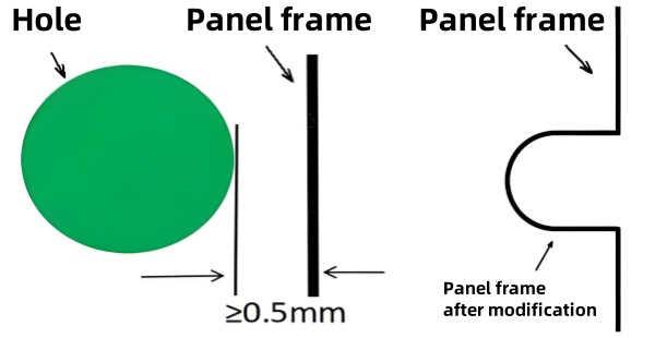
(1) The minimum distance from a through-hole to the board frame line is 0.5mm. If less
than 0.5mm, it should be changed to a U-shaped hole (the hole is connected to the board
frame).
(2) The distance from a via
to the solder mask opening should be at least 0.2mm; otherwise, copper may be exposed at
the hole edge.
(3) It is not
recommended to design vias-in-pad for FPC. FPC cannot perform resin plugging, and
vias-in-pad may cause solder leakage.

(1) Oxidation of large copper surfaces: Due to the design of large
copper surfaces, air is difficult to evacuate during film lamination. Moisture in the
air reacts with the copper surface under high temperature and pressure to cause
oxidation, resulting in poor appearance (functionality is not affected). To avoid this,
design grid copper cladding or add solder mask openings on large copper surfaces.
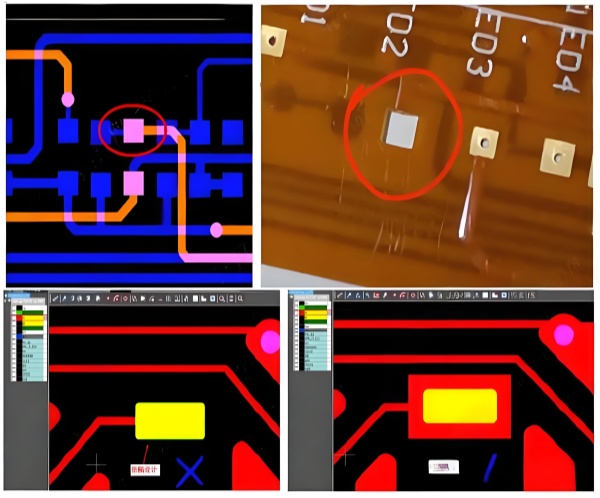
(2) Avoid independent
solder pads: As shown in the figure, circuit solder pads that are independent
and overlapping on both sides are prone to detachment (since the intermediate substrate
of FPC is only 25μm). It is recommended to add copper cladding, connect the four corners
of the pads to the copper cladding with connecting lines, and stagger the upper and
lower pads to increase bonding strength.

(3)
Pad detachment: Connector seat pads are relatively independent and
prone to detachment; use pressed PAD design.
(4) Avoid large areas of exposed
copper, as this may cause wrinkles.
(5) FPC uses coverlay as the
solder mask layer. The coverlay needs pre-opening and bonding. There should be a 0.2mm
spacing between the solder pad and the trace, and the solder mask bridge should be at
least 0.5mm (i.e., the spacing between two solder pads should be at least 0.5mm).
Otherwise, open a full window and accept exposed traces.
(6)
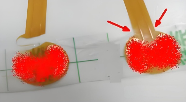
Tearing at
corners: Sparse cable traces make corners prone to tearing. Add anti-tear
copper strips on the board edge or grid copper on the back.

(7) The circuit grid is preferably laid at a 45-degree angle for better signal
transmission. The recommended line width and spacing are 0.2/0.2mm.
(1) For pluggable fingers: High-temperature carbonization at the board edge during laser
cutting may cause micro-shorts between gold fingers. The gold fingers need to be
recessed by 0.2mm (generally uniformly recessed; special requirements should be
specified).
(2) For soldering
fingers: Vias on the in-board solder pads should not be arranged in a single row to
prevent stress concentration and breakage.
(3) The upper and lower coverlays
of soldering fingers should be staggered by more than 0.3mm to prevent breakage.
(4) Soldering fingers are
recommended to have a solder mask film pressing PAD effect (i.e., extend the solder pad
so that the coverlay presses the pad by more than 0.3mm).
(5) Solder mask opening for gold
fingers: The opening is recommended to press the pad by more than 0.3mm to prevent
disconnection between the gold finger PAD and the connection.
(6) If hollow boards are not
supported, reverse fingers need to add pads and vias to achieve layer change.
(7) Since FPC solder mask film
cannot form solder mask bridges like green oil, IC-type pads should have no extra copper
cladding (unreasonable design may cause soldering short circuits due to larger pads and
reduced spacing).
(8) Gold finger
pads should be independent; copper cladding or traces on finger pads will be exposed
after solder mask opening.
(9) The
default tolerance for gold finger outline is ±0.1mm; ±0.05mm requires confirmation when
placing an order.
(1) FPC connector seats are prone to detachment; use pressed PAD design.
(2) Bridging is required in the
middle of the IC to retain the intermediate solder mask.
(3) Gold finger pads must have
solder mask openings; otherwise, they cannot conduct with the connector.
(4) Soldermask is used as the
default solder mask layer; ensure the correctness of the solder mask layer.
(5) To prevent via copper from
breaking during bending, FPC vias are generally defaulted to be oil-covered; opening
requires notation when placing an order.
(6) Test points designed as via
attributes may not be transferred correctly; avoid via attributes or set separate
openings.
(7) Large exposed copper
gold surfaces on the edge of double-sided boards may cause edge blackening; add a circle
of coverlay on the board edge.
(1) If there are character silk screens on the stiffener, select "silk screen on
stiffener" when placing an order to prevent process errors.
(2) Instruction text should not be
designed inside the board to avoid issues in subsequent processes.
(1) For boards with steel stiffeners: The minimum spacing between boards is recommended
to be 3mm, the slot width is 0.5mm, and the connection point width is 1mm (one added
every 15mm or so). Note when placing an order: Separate each piece with paper, and ship
with cardboard clamping top and bottom.
(2) Panelization connection
positions on gold fingers will cause uneven front ends of gold fingers.
(3) Too few connection points
cause boards to fall off easily; each PCS should have at least 2 connection points
(width 0.8mm), with more for larger boards.
(4) For small boards without SMT:
Each PCS only needs 2 connection points of 0.3mm for easy hand-breaking.
(5) Low panelization utilization
leads to high quotations; optimal panel widths are 119mm or 240/250mm; third-party
panelization is recommended.
(6)
Boards smaller than 20×20mm may be sucked away by laser dust suction; deliver panels or
depanelize after production.
Stiffening of flexible circuit boards refers to adding rigid materials to local areas of
FPC to facilitate assembly. PI stiffeners are suitable for gold finger pluggable
products; FR4 for lower-end products; steel sheets (good flatness, no deformation) for
chip mounting products. See details in the Stiffener Specification Diagram.
(1) Avoid steel sheets as stiffeners for component insertion holes (risk of short
circuits), with Hall elements (weak magnetism), or for pluggable gold fingers.
(2) For pluggable gold fingers,
note total thickness requirements (specified in connector specifications); PI stiffener
thickness is not directly calculated by subtracting FPC board thickness from total
thickness.
(3) Stiffener opening
design: Avoid underlying component holes or pads (customer design is preferred; default
avoids pads by 0.3mm). Stiffeners with remaining width <2mm after cutting are
omitted.
(4) The height of the gold
finger stiffener should be at least 1.0mm longer than the gold finger pads to prevent
breakage.
(5) Electromagnetic film
with conductive sides: Cancel design if the lower film is not a single network.
(6) For electromagnetic film
grounding resistance requirements: Customer designs independent grounding solder mask
openings (default adds >1.0mm windows randomly). Note: Ungrounded electromagnetic
film may cause signal problems; prototyping and verification are necessary.
(7) Attaching steel sheets to
solder pads causes short circuits.
(8)
Stiffener width: FR4 stiffeners with width <5mm are prone to breakage and
carbonization; change to PI or steel stiffeners. Adhesive backing minimum width >3mm.
(9) No stiffeners or adhesive
backing around chip mounting pads (prevents solder paste printing); chip mounting should
precede stiffener/adhesive backing attachment if necessary.
The board thickness includes the coverlay, copper thickness, and substrate PI thickness.
Boards with copper-free areas or no coverlay have correspondingly reduced thickness; pay
special attention during design.
 03 Jun 2025 15:48:06 GMT
PCBASAIL
