BGA PCB Design Tips: Rules, Routing & Layout Guide
When integrated circuits are cut from silicon wafers, they can be packaged in many different ways. These include Dual In-line Package (DIP), Small Outline Integrated Circuit (SOIC), Thin Quad Flat Package (TQFP), Quad Flat No-leads (QFN), and Ball Grid Array (BGA).
In different plastic packages, the connection between the silicon IC and the package pins is made using a technique called wire bonding.
DIP packages are larger and easier to solder by hand (better for hobbyists). BGA packages, however, cannot be soldered by hand. They need special equipment to be assembled onto a PCB.
BGA packages have the highest pin density. This means they take up the smallest amount of space on a PCB. This is essential for most modern high-end electronic products, such as smartphones. Yet, having such high density means special techniques are needed to route all signals onto the PCB.
Below are some general tips for routing BGA chips during the PCB design process.
Design Rules
Even before starting the PCB layout, the first step is to set the design rules.
- How many layers will the board have?
- What is the minimum track width?
- What is the minimum track spacing?
- What is the minimum via size (minimum drill diameter and minimum annular ring)?
In general, more layers and smaller feature tolerances make it easier to route the circuit board. But more layers and tighter tolerances usually make the board more expensive (and slower to manufacture).
Product Volume
One deciding factor is the expected product volume – how many of these boards are projected to be made? For high-volume products, it may be worth putting in extra effort to route carefully using as few layers as possible. This helps lower the cost per PCB. For low-volume products, though, the labor cost of spending extra time to route to fewer layers is not reasonable.
It is also necessary to check the capabilities of your PCB manufacturer. You need to make sure they can actually produce boards that meet your design specifications. This includes their minimum trace width, trace spacing, drill size, and annular ring specifications (as well as the maximum number of layers they can produce).
Impedance Requirements
Another factor is impedance requirements. You need to consider if any (or many) traces need a specific impedance. Trace width, trace spacing, and the layer stack will determine the trace impedance. Also, it goes without saying that some inner layers of the board will be power reference layers (for constant impedance). Check our high-speed design articles if you are not familiar with this.
Some BGAs (like Microprocessor Units (MPUs)) have multiple power domains. The power layers in the inner layers of the board are usually divided into different sections. This is based on the power connections used by specific areas of the chip. For example, DDR memory may operate at a specific voltage. It will have power planes that span the DDR chip and the DDR section of the MPU. The SD/eMMC section, on the other hand, will operate at a different voltage. It will have its own power planes that span that memory and the corresponding section of the MPU.
Having the correct power layer under the related pins is important for impedance matching. It also makes routing these pins easier. They only need a via down to the power layer (instead of a trace routed outside the BGA area).
Component Documentation
Sometimes, IC data sheets offer suggestions on design rules. For example, there is an excerpt in STMicroelectronics' STM32MP1 application note about getting started with hardware design for that processor.
Example of design guidelines from an IC data sheet
In general, it is a must to check any design requirements or suggestions in the component documentation. There may also be specific design constraints for routing certain parts of the design. For example, there are impedance and spacing requirements for DDR connections.
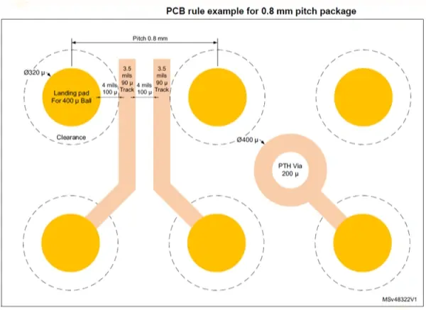
When extracting PCB footprints from libraries, it is necessary to check the BGA pad sizes of the imported components. Generally, these sizes should be 80% of the BGA ball diameter. But this is not always set correctly when importing the footprint.
BGA chips almost always need decoupling capacitors. They may also need calibration resistors placed close to the chip (usually right under it). So, determining the package sizes of these capacitors is an important step that should be done in advance. Also, smaller package sizes make routing easier. But they require more advanced (and possibly more expensive) equipment and processes for PCB assembly.
Another source to check when deciding on design rules is the chip's reference design board. No matter what PCB design software is used, manufacturers usually provide board Gerber files. These can be opened and checked using Gerber viewing software like ViewMate. You can check the number of layers, track width, track spacing, and via size.
Via Options
Another potential design decision is whether to use blind vias and/or buried vias. These are also more expensive. But they make higher-density designs easier (and even possible). Pad via technology is another option that can be used to increase density. But it also costs more.
Routing Placement
Another source to check when deciding on design rules is the chip's reference design board. No matter what PCB design software is used, manufacturers usually provide board Gerber files. These can be opened and checked using Gerber viewing software like ViewMate. You can check the number of layers, track width, track spacing, and via size.
Some BGAs have selectively filled balls. Some ball positions on the BGA are not used. This creates escape routes for routing tracks.
Removing non-functional pads on inner-layer vias helps free up more routing space (when using boards with 6 or more layers).
Vias are usually arranged in a dogbone pattern.
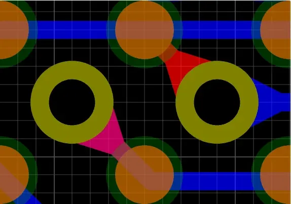
Example of a dogbone via pattern for BGA routing
A technique to increase the density of traces escaping from inner rows is to arrange vias in a way that creates a channel. In this channel, multiple traces can be routed very close together.
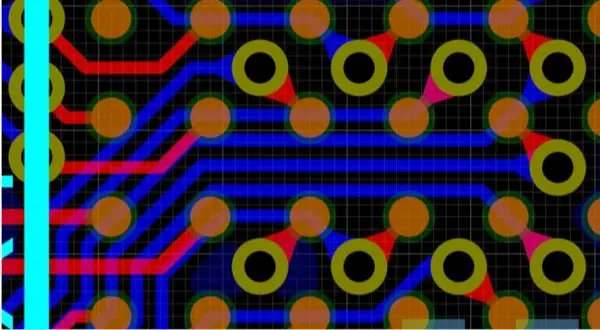
Channel routing technique for inner row traces
As a final tip, it can sometimes help not to place adjacent chips (like an MPU and DDR) too close. This leaves enough space for length-matched serpentine traces. These traces often take up more space than you might think.
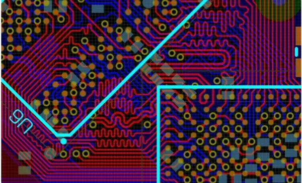
Length-matched serpentine traces between adjacent chips
Need a PCBA Quote?
Get professional pricing for your BGA PCB assembly project. Our experts can handle complex designs with high-density components.
Request PCBA QuoteFast turnaround quotes (within 24 hours)
BGA assembly specialists
No obligation on initial quotes