A Simple Guide to EMC Design in PCBs
 25 Apr 2025 14:19:44 GMT
PCBASAIL
1. Layer Stack-Up
1.1 Layer Setup
In PCB EMC design, the first step is to determine the layer stack-up. The board’s layers include power planes, ground planes, and signal layers. The placement and splitting of these planes directly impact EMC performance.
1.2 Choosing Number of Layers
The number of layers is determined by factors such as:
- Number of power rails required
- Number of ground areas needed
- Signal density and quantity
- Operating frequency of the board
- Number of nets requiring special routing (e.g., high-speed signals)
- EMC targets (e.g., CISPR16 Class B)
- Budget
If EMC requirements are high and cost permits, adding extra ground planes can enhance EMC performance.

1.3 Power Plane Count
- For a single power rail, use one power plane.
- For multiple non-overlapping rails, split a single plane into regions. Ensure nearby signal layers do not cross these splits.
- For overlapping rails, use two or more separate planes. Each plane must serve only its designated rail, and critical signals must not cross splits.
1.4 Ground Plane Count
In addition to matching power requirements, ground planes must:
- Be placed directly under components (e.g., Layer 2 or the second-to-last layer).
- Adjacent to high-speed or clock signal layers.
- Adjacent to each power plane (e.g., 48 V power plane next to a ground plane).
1.5 Signal Layers
Use your CAD tool’s routing density report to estimate the number of signal layers needed, then adjust based on frequency, special nets, EMC goals, and cost. Ensure key nets and vulnerable nets are shielded by adjacent planes.
2. Plane and Signal Placement
2.1 Power–Ground Impedance
Both power and ground planes have inherent impedance, with power planes typically having higher impedance. Placing each power plane directly adjacent to its corresponding ground plane reduces impedance. Together with decoupling capacitors, these plane pairs provide a broad decoupling bandwidth, though they may resonate.
2.2 Reference Plane
Both power and ground can serve as reference planes, but ground is preferred because it is tied to earth and offers better shielding. Whenever possible, use the ground plane as the reference.
2.3 Stack-Up Rules
Once the number of layers is determined:
- Layer 2 (under components) should be a ground plane.
- Every signal layer must be adjacent to a ground plane.
- Avoid placing two signal layers back-to-back.
- Each power plane must be adjacent to its corresponding ground plane.
- Maintain a symmetric stack-up to prevent warping.
For motherboards operating above ~50 MHz:
- Use full ground planes on the top and bottom layers.
- Do not place two routing layers consecutively.
- All routing layers must be adjacent to ground planes.
- Ensure key nets stay adjacent to ground planes and do not cross splits.
Apply these rules flexibly, adapting to specific design needs.
3. Module Division & Component Placement
Effective EMC layout requires clear module zoning and proper component placement.
3.1 By Function
Group circuits by their role (e.g., clock, amplifier, driver, A/D-D/A converter, I/O, power, filter). Arrange zones to ensure short signal flow and avoid mixing different module types.
3.2 By Frequency
Separate high-, medium-, and low-frequency modules into non-overlapping areas.
3.3 By Signal Type
- Keep digital and analog zones isolated.
- Place A/D and D/A components at the boundary between zones.
- Orient analog pins toward the analog ground and digital pins toward the digital ground.
- Keep traces for these components short.
4. Layout Tips
- Follow signal flow: Prioritize short trace lengths, even if the layout appears less neat.
- Clock nets: Keep them extremely short or shield them with ground planes on both sides. Keep clocks away from analog components, I/O ports, and connectors.
- Low-speed I/O & analog I/O: Place near connectors.
- High-speed logic, clocks, and memory: Position deep inside the board, away from edges.
- A/D & D/A converters: Place near the board’s center to minimize trace length.
Key Points
- Define distinct zones for digital, analog, clock, power, and I/O.
- Place converters at zone boundaries with correct pin orientation.
- Position clocks, high-speed components, and memory far from board edges.
- Short traces are more critical than layout neatness.
- Keep power drivers away from splits and route them directly off the board.
- Place oscillators and crystals close to their associated ICs.
- Keep reference voltage sources away from digital nets.
5. Special Part Placement
5.1 Power Modules & DC/DC
Place at the board’s power entry point to reduce EMI in supply lines. Keep traces short and isolate this area using via fences or split lines.
5.2 Clock Generators
Position away from edges and connectors. Route clock signals on inner layers and keep them short.
5.3 Inductors & Coils
Keep away from high-speed or sensitive traces. If necessary, align their planes to minimize magnetic coupling.
5.4 Bus Drivers
These components radiate significantly—keep them away from board edges and place them close to their connectors. Use local shields if multiple drivers are present.
5.5 Filters & Decouplers
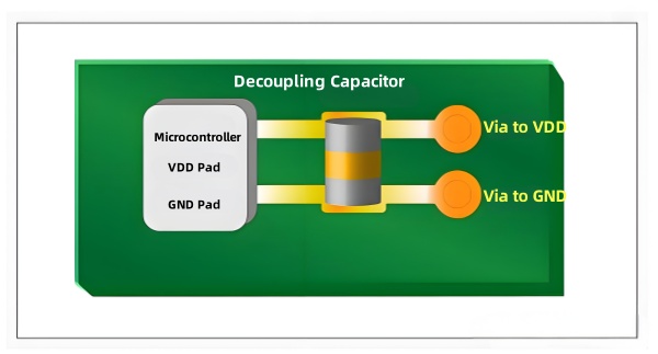
- Place decoupling capacitors directly at IC power pins.
- Position input/output filters at connectors.
- Place module filters at the module entry point.