A Complete Guide to COB Packaging and Bonding Techniquess
Description of Chip On Board (COB) Packaging
Chip On Board (COB) packaging is a technology where a semiconductor chip is directly mounted on a printed circuit board (PCB). The electrical connection between the chip and the substrate is achieved through wire bonding. After connection, the chip is covered with resin to ensure reliability.
The COB process starts with applying a thermal conductive epoxy resin (usually epoxy mixed with silver particles) to the area on the substrate where the silicon chip will be placed. The silicon chip is then directly placed on this surface. It is heated until the chip is firmly fixed to the substrate. Next, wire bonding is used to establish a direct electrical connection between the silicon chip and the substrate.
Advantages
- Low cost (about one-third of other methods)
- Space-saving design
- Mature manufacturing process
- Improved IC signal performance
- Reduced parasitic components
Disadvantages
- Requires specialized equipment
- Potential speed limitations
- Stringent environmental requirements
- Non-repairable nature
- Potential thermal expansion issues
Technical Insight
Some COB layouts can improve IC signal performance by removing most or all of the packaging, which eliminates most parasitic components. However, substrate connections to VCC or ground may suffer due to lead frames or BGA markers, potentially causing thermal expansion issues and poor substrate connections.
What is COB Soft Packaging?
COB soft packaging is a semi-closed small packaging technology and a common electronic packaging method. COB stands for Chip-on-Board, meaning the chip is mounted directly on the circuit board. The main features of COB soft packaging include good sealing, small size, low packaging cost, and high reliability. Its main role is to provide a reliable packaging and connection method, protect sensitive electronic components, and provide functions such as connection, electrical isolation, and heat dissipation.
Features and Main Functions of COB Soft Packaging
Key Features
Good Sealing
One feature of COB soft packaging is good sealing. COB technology attaches the chip directly to the substrate. It uses packaging materials to seal the chip and circuits. This forms a structure that effectively resists dust, moisture, and vibration. This packaging method protects the chip well. It improves the chip’s stability and reliability.
Small Size
COB soft packaging has a small size. COB technology allows the chip to be very close to the circuit board. This reduces the packaging volume. The small size is ideal for integrating more functions and components in limited space. It improves the overall performance of the circuit.
Low Cost
COB soft packaging has relatively low costs. COB technology does not require additional packaging components. It only uses suitable packaging materials to connect the chip and the circuit board. So, the cost is lower. Also, because of its small size, it reduces material and assembly costs.
High Reliability
COB soft packaging has high reliability. The chip is directly attached to the circuit board and sealed with packaging materials. This creates a stronger and more stable connection. This method reduces wire lengths and connectors. It lowers the vulnerability of connection points. This improves the stability and reliability of the circuit system. Moreover, COB soft packaging provides better heat dissipation. It ensures the chip does not overheat during operation. This extends the chip’s lifespan.
Main Functions
Reliable Packaging
In modern electronic devices, chips are very important. COB technology attaches the chip directly to the circuit board. It seals the chip with suitable materials. This protects the chip from the external environment. It prevents damage from dust, moisture, and vibration. It improves the chip’s reliability and stability.
Circuit Connection
COB technology uses proper circuit design and packaging materials. This connects the chip to other components on the circuit board. It enables signal transmission and power supply. At the same time, COB soft packaging uses suitable isolation materials to achieve electrical isolation. This ensures the circuit’s stability and safety.
Electrical Isolation
COB technology uses proper circuit design and packaging materials. This connects the chip to other components on the circuit board. It enables signal transmission and power supply. At the same time, COB soft packaging uses suitable isolation materials to achieve electrical isolation. This ensures the circuit’s stability and safety.
Heat Dissipation
COB soft packaging also has a heat dissipation function. The chip is very close to the circuit board. So, COB technology can effectively conduct heat from the chip to the circuit board. It then dissipates the heat through heat dissipation designs. This keeps the chip within a normal operating temperature range. It avoids overheating, which can harm performance and lifespan.
In summary, COB soft packaging is a semi-closed small packaging technology. It has features like good sealing, small size, low cost, and high reliability. Its main roles are to provide reliable packaging and connection, protect sensitive components, and offer connection, electrical isolation, and heat dissipation. This packaging method is widely used in modern electronic devices. It provides important support for the performance and reliability of electronic products.
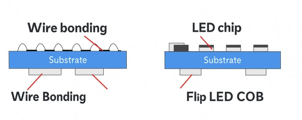
Differences Between Front-Mounted and Flip-Chip COB Packaging
COB packaging includes front-mounted COB and flip-chip COB. Front-mounted COB has limitations in product performance development. These come from its light-emitting angle and wire bonding distance. Flip-chip COB is an upgraded version of front-mounted COB. It builds on the front-mounted COB’s advantages: ultra-small pixel pitch, high reliability, and surface light emission. It further improves reliability, simplifies production processes, enhances display effects, offers perfect near-screen experience, and achieves true chip-level spacing, reaching Micro levels.
Comparative Analysis
| Feature | Front-Mounted COB | Flip-Chip COB |
|---|---|---|
| Connection Method | Wire bonding | Direct bonding (wire-free) |
| Welding Area | Point contact | Surface contact |
| Packaging Thickness | Thicker (accommodates wires) | Thinner (no wire space needed) |
| Pixel Pitch | Limited (≥1.0mm typically) | Ultra-small (Micro levels, <1.0mm) |
| Reliability | Good | Excellent (fewer solder joints) |
| Power Consumption | Higher | 45% lower at same brightness |
| Thermal Performance | Good | Superior (10°C cooler at same brightness) |
PCBASAIL’s Flip-Chip COB Advantages Over Front-Mounted COB
Key Technical Specifications
Ultra-High Reliability
Jingrui Chuangxian’s full flip-chip COB products use full flip-chip light-emitting chips and wire-free packaging processes. The light-emitting chips are directly bonded to the pads on the PCB. The welding area changes from points to surfaces, increasing the welding area. It reduces the number of solder joints. This makes product performance more stable. The packaging layer has no space for wires, making it thinner and lighter. This reduces thermal resistance, improves light quality, and extends the display’s lifespan. It also has ultra-high protection: anti-collision, anti-vibration, waterproof, dustproof, anti-smoke, and anti-static.
Excellent Display Effect
PCBASAIL’s full flip-chip COB, as an upgraded product of front-mounted COB, has a thinner packaging layer. This completely solves the problem of color lines and bright/dark lines between front-mounted COB modules. It has an ultra-high contrast ratio of 20000:1 and a peak brightness of 2000CD/㎡. The black levels are darker, the brightness is higher, and the contrast is better. It supports HDR digital image technology, ensuring fine and perfect static and high dynamic image quality.
Ultra-Small Pixel Pitch
Full flip-chip COB uses chip-level packaging. It does not require wire bonding. Its physical size is only limited by the size of the light-emitting chip. This breaks the pixel pitch limit of front-mounted chips. It is the first choice for products with a pixel pitch below 1.0.
Ultra-Energy-Saving and Comfortable
Full flip-chip light-emitting chips reduce power consumption by 45% under the same brightness. The active layer is closer to the substrate, shortening the heat flow path from the heat source to the substrate. This results in lower thermal resistance. The flip-chip occupies a smaller area on the PCB. This increases the substrate’s duty cycle, providing a larger light-emitting area. The light-emitting efficiency is higher, and the screen surface temperature is significantly reduced. Under the same brightness, the screen surface temperature is 10℃ lower than that of conventional front-mounted chip LED displays.
Main Welding Methods for COB
Thermocompression Welding
This method uses heat and pressure to weld metal wires to the welding area. The principle is: heat and pressure cause plastic deformation in the welding area (such as aluminum). This breaks the oxide layer on the welding interface. Then, atomic attraction forms a “bond.” Also, the uneven surfaces of the two metals allow them to interlock when heated and pressed.
This technology is generally used for Chip On Glass (COG) on glass plates.
Ultrasonic Welding
Ultrasonic welding uses energy from an ultrasonic generator. A transducer rapidly expands and contracts under ultra-high frequency magnetic induction. This produces elastic vibrations. These vibrations are transferred to the wedge tool. At the same time, a certain pressure is applied to the wedge tool. Under these two forces, the wedge tool drives the aluminum wire to rub rapidly on the metallized layer (such as an aluminum film) of the welded area. This causes plastic deformation on the surfaces of the aluminum wire and aluminum film. The deformation breaks the oxide layer on the aluminum interface. The two clean metal surfaces come into close contact, forming an atomic bond and thus welding.
The main welding material is an aluminum wire welding head, usually wedge-shaped.
Gold Wire Welding
Ball bonding is the most representative welding technology in wire bonding. This is because modern semiconductor packaging and transistor packaging use gold (AU) wire ball bonding. It is easy to operate, flexible, and has strong solder joints (the welding strength of a 25UM gold wire is generally 0.07–0.09N per point). It has no directionality. The welding speed can reach more than 15 points per second. Gold wire welding is also called thermal (pressure) (ultra)sonic welding
The main bonding material is gold (AU) wire, and the welding head is spherical, so it is called ball bonding.
COB Packaging Process
Step-by-step manufacturing workflow for Chip On Board packaging
Step 1: Wafer Expanding
Use an expander to evenly expand the entire LED chip film provided by the manufacturer. This spreads out the closely arranged LED chips attached to the film surface, making die bonding easier.
Creates space between densely packed chips for easier handling in subsequent processes
Silver paste ensures optimal thermal and electrical conductivity between components
Step 2: Back Gluing
Place the expanded wafer ring on the surface of a back gluing machine that has been coated with a silver paste layer. Apply silver paste to the back. Dot silver paste. This is suitable for bulk LED chips. Use a dispenser to apply an appropriate amount of silver paste to the PCB.
Step 3: Die Bonding
Put the wafer ring with silver paste into a die bonding frame. An operator uses a die bonding pen to place LED chips on the PCB under a microscope.
Precision placement under magnification ensures accurate component positioning
Controlled temperature curing creates strong bonds while preventing component damage
Step 4: Silver Paste Curing
Put the PCB with die-bonded chips into a thermal cycle oven. Let it stand at a constant temperature for a period. Take it out after the silver paste is cured. Do not leave it for too long. Otherwise, the LED chip coating will turn yellow (oxidize), making bonding difficult. If there is LED chip bonding, these steps are needed. If only IC chip bonding is done, these steps are skipped.
Remaining Process Steps
Chip Mounting
Use a dispenser to apply an appropriate amount of red glue (or black glue) to the IC position on the PCB. Then use anti-static equipment (vacuum pen or tweezers) to place the IC bare chip correctly on the red or black glue.
Drying
Curing adhesive in thermal Put the mounted bare chip into a thermal cycle oven. Place it on a large flat heating plate and let it stand at a constant temperature for a period. It can also be cured naturally (which takes longer).
Bonding (Wire Bonding)
Establishing electrical Use an aluminum wire bonding machine to bridge the chips (LED chips or IC chips) with the corresponding pads on the PCB using aluminum wires. This is the inner lead welding of COB.
Pre-Testing
Initial electrical Use special testing tools (different COB uses different equipment; a simple one is a high-precision regulated power supply) to test the COB board. Rework unqualified boards.
Dispensing
Applying protective Use a dispenser to apply an appropriate amount of mixed AB glue to the bonded LED chips. ICs are packaged with black glue. Then, perform appearance packaging according to customer requirements.
Curing
Final curing of Put the glued PCB into a thermal cycle oven. Let it stand at a constant temperature. Different drying times can be set according to requirements.
Post-Testing
Final electrical Test the packaged PCB again with special testing tools for electrical performance. Classify the good and bad products.